Continue to Site
Follow along with the video below to see how to install our site as a web app on your home screen.
Note: This feature may not be available in some browsers.
So unfortunately, it might be possible that it is impossible to have a transparent conductor.
Current does tend to take the path of least resistance. But it does "leak out". For example, a large flat square with two tiny contacts at opposite corners. THe current will for the most part flow in a straight line, but it does kind of spread out around the middle before converging to get to the opposite contact. And you will probably find exponentially less current flowing through the metal as you move farther away from this line.
Same deal goes for current flowing a flat copper sheet, and then a flat sheet with a block of copper sitting in the middle. Small amounts would flow through the copper block, but very little. Even less if it was farther away from "the line" between the contacts on the copper sheet.
I think somebody else on the forum in another thread a while back brought up carbon sheets (like carbon paper) and is a flat resistive material with documented resistances. CAn't say whether or not it would work for whatever application you are looking for.
Carbon paper might work, but I would prefer something more durable… Are there simple models of the electrical properties of conductors that have an inconsistent composition of more than one semi-finished material, like a geometric model of electron flow?
Are there simple models of the electrical properties of conductors that have an inconsistent composition of more than one semi-finished material, like a geometric model of electron flow?
..If you are looking to map the distribution of electron flow through something, that is something essentially "no one" really cares about....
A fire investigator might be interested in the range of resistances of slabs of material – though these slabs of material might not be made for the purpose of measuring resistances.
How so, do you think?
Is this still all about your game board?
As pointed out earlier, even if you had such a material how would you determine more than one game piece's location? or for that matter how do you make an X-Y resistive sheet? Your game piece would have to connect across a grid to indicate it's position.
If what you are looking for is a large hard slab of resistive material, you're out of luck. You'd have to approach a resistor manufacturer and custom order large slab-like resistors that are made of some resistive ceramic or resistive or alloy which would be very very expensive and they wouldn't even consider you because you aren't ordering in massive quantities. One of the problems is that the more material you have, the smaller the resistance and the harder it gets to measure. Another problem is you need the resistive material exposed (when it is normally coated for protection in resistors) and they tend to be materials that aren't so durable.
Huh? If you are looking to map the distribution of electron flow through something, that is something essentially "no one" really cares about. And anyone that did would be using electromagnetics simulation software to do it. The rarity of software like that would probably make it very expensive too. How would you even pin point where something is on a single resistive sheet?
I'm going to try now to convince you to consider alternative methods:
1. Did you think of your physical circuit implementation to detect something on a resistive sheet? The only way I can come up with is to line the edges of the sheet with contacts and then measure the resistance between every single opposing pair of contacts and then choose opposing X-pair with the lowest resistance and the Y-pair with the lowest resistance and call that the position of the playing piece. A few problems arise with this method. First of all, it is IMPOSSIBLE to detect the position of more than one piece because there is just too much coupling between the outputs and the positions of the pieces. This pretty much puts the nail in the coffin for a gaming board.
2. Playing pieces tend to be much smaller than the board itself (by definition almost), and since current distributions decrease exponentially away from the line of sight between the two contacts that are conducting current, this means that for the most part, the height of a playing piece does not contribute very much to current flow. At the same time, it also means that you are not forcing current to flow across the piece and the patch of board it is in contact with. Current is still free to leak flow around the piece on the board and both of these effects means the change in resistance produced is even less.
3. Also by definition, one board tends to have a large number of playing pieces. Recall that resistors of largely different values tend to dominate each other in different ways when connected in series or in parallel. A parallel connection would be similar to the playing piece and the patch of board it is in contact with, and a series connection would be this patch/piece and the REST of the board. This means that either way, you cannot have a large difference in "effective resistance" (taking into account how current will now flow through the entire volume of the playing piece and how current will also flow on the board around the piece) between board and piece. That's somewhat of a problem seeing as how you have many different playing pieces. Dividing the board's resistance up equally among the playing pieces doesn't work because as soon as you split the piece/patch resistor pairs, you get the board-only paths dominating the resistance circuit. More smaller footprints for each piece also means more leakage current around the piece compared to one large piece of the same combined footprint. It just doesn't work.
From your previous thread, it seems you are just going about this the wrong way and seem unopen to alternative methods. Lots of people come onto the forums with great difficulty finding parts or designing things because they are going about things the wrong way and continue to have difficulty because chose an approach that isn't possible with current materials or technology and refuse to change. Things for such applications do exist. Like capacitive touch, or really any array of anything- resistive, capacitive laser, etc. They also have the advantage of durability especially capacitive since it works through materials unlike resistance which needs direct contact.
But I think the most important change that is needed is for you to use an array of elements rather than a single array (plus it will be a lot easier to get a bunch of smaller parts than one really big part). Well, that's not entirely true. Your own camera suggestion from your previous thread probably counts as single element unless you count the CCD pixels. But that is probably the best way if you have too many elements in your array to build. If only to be able to detect the position of more than one piece. If you really want a "simple model" one good guess is that it is a gaussian distribution away from the line between the two contact points, even then this does not change the arguments made above.
I have been watching this thread and I need you to clarify this for me.
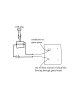
To simplify things lets look at the problem in one dimension instead of two. It can be easily modeled with a variable resistor. The voltage of on the wiper in respect to ground indicates where the wiper is on the resistor.
The problem is "in respect to ground". A game piece has no ground. Even if it did how are you going to get a signal back to whatever it is that will read it?
How large is the play area ?