Electro Tech is an online community (with over 170,000 members) who enjoy talking about and building electronic circuits, projects and gadgets. To participate you need to register. Registration is free. Click here to register now.
Welcome to our site! Electro Tech is an online community (with over 170,000 members) who enjoy talking about and building electronic circuits, projects and gadgets. To participate you need to register. Registration is free. Click here to register now.
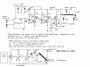
The thumbnail gives a pretty good basic layout for the parts and trace routing.
Make trace widths minimum to minimize capacitance (except for the connection from the output transistor to antenna as shown).
Lay out to minimize trace lengths.
Make sure to add the vertical grounded copper screen (shield) shown between stages to minimize the chances of oscillation.
Use a ground plane on the component side of the board as shown.
Connect all decoupling capacitors directly to the ground plane (surface mount caps are best)
And, as with all HF circuit design, good luck.
I would stress that you should follow the layout and components given by the inventor/author. The components are likely tweaked for the circuit to operate best based on that layout.
Your board would best work using a microstrip layout. Trace width should be chosen based on impedance. In your case I think 75 ohm. Read up on microstrip, and you can also get some info here.
This site uses cookies to help personalise content, tailor your experience and to keep you logged in if you register.
By continuing to use this site, you are consenting to our use of cookies.