Continue to Site

Welcome to our site!

Electro Tech is an online community (with over 170,000 members) who enjoy talking about and building electronic circuits, projects and gadgets. To participate you need to register. Registration is free. Click here to register now.

  • Welcome to our site! Electro Tech is an online community (with over 170,000 members) who enjoy talking about and building electronic circuits, projects and gadgets. To participate you need to register. Registration is free. Click here to register now.

Turning a joystick pot control into voltage control inputs

Status
Not open for further replies.

melittophily

New Member
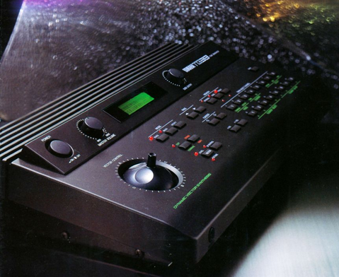
So I am looking to modify a music synthesizer here:

d3845cc22f367f604dcad6d2797ff2ff.png

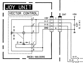
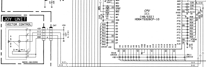
It seems clear: the +5VDC voltage source splits and goes through two 10k pots in voltage divider configuration with the middle pins respectively leading to V-X and V-Y, with a range of 0-5V, both passing through a 1k resistor and a 0.01uF cap to ground before reaching the CPU analog input pins. So a 0-5VDC control voltage signal from other synthesizer gear (LFOs, envelopes, etc) coming from a 1/8" TS jack (hot tip, ground sleeve) should be able to stand in for it.

Now this is where I feel like an idiot: I'm unsure about the cleanest way to wire up switching on this. The switching scheme is:
x jack tip signal vs x pot middle pin to V-X [then to CPU]
y jack tip signal vs y pot middle pin to V-Y [then to CPU]

I take it I should break the signal coming from the middle pin of the joystick pot and wire that into one side of the switch on a NC switching 1/8"/3.5mm jack, with the other side of the switch merged to the tip signal and going back to V-X/Y on the joystick assembly -> CPU.

Now, when thinking about this, it occurred to me that with something plugged in, it could leave the joystick discharging +0-5V to a shared ground and I'm wondering if that might cause problems. Should I use a jack that leaves the switch floating instead of grounded if something is plugged in? Maybe I'm overthinking it.

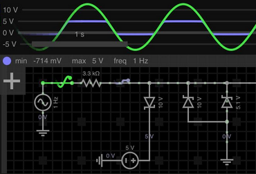
Lastly, protection. I assume a diode to block negative voltages would be a good idea. For overvoltage, would a 5V zener or schottky from tip to sleeves on the input jacks work? Most of the frequencies I use around the studio max out at 5V or a little above but accidents do happen and I don't want to fry the CPU.

I'd rather go direct than use optoisolators and have to convert input voltage to LED current to resistance back to voltage and get a slow finnicky response. I assume the R-C filter there will pull out frequencies that could harm the chip and the joystick has always had a good response to being jerked around quickly. So while isolation through a vactrol/coupler is often the safest route, it just makes the job more complex than it probably needs to be here as long as the overvoltage protection works.
 
Last edited:
Welcome to ETO, melittophily!

Can you provide some of the circuit into which you are feeding the joystick signal(s)?

Is the 5VDC source that unstable that you need the level(s) of protection you describe?
 
Thank you for the welcome and taking the time to read!

The main voltage sources I would use would be the low frequency oscillator and envelope CV outputs from my Arturia Microbrute analog semi-modular synth. They're fairly stable 0-5Vish DC control signals coming from shielded 1/8" tip-sleeve cables.

Another one I would like to carefully use is a more complicated situation using Expert Sleepers Silent Way plugin suite and some extra circuitry to turn signals in my digital audio workstation software (Ableton Live) and audio interface into DC control voltages. This provides software LFOs, envelopes, V/Octave pitch control, gates, pulses, etc. for analog synth/effects/etc devices.

So these other modular components would be able to control what is normally the X and Y of the joystick - switchable between vector mixing of 4 waveforms, or pitch detuning. This should blow the creative possibilities of this synth through the roof for me. I already successfully use these signals into the expression pedal inputs of effects units and use the Silent Way plug-ins to make more complex sounds on the hardware Microbrute.

The CV is intentionally variable to allow sounds to evolve over time and given the nature of analog I guess it always has some degree of instability (sometimes desired, musically) Full modular systems frequently use 10V signals but in both cases I am using inexpensive solutions where the signals are lower - though occasionally hitting ~5.5V to 6V by my measurements. I have resistor/pot passive attenuators and diodes built into 1/8" cables for various tasks, but in this project I don't want to full-time limit the full 0-5V sweep going into the vector control if I can reliably keep anything below 0 or above 5V from getting to the CPU. Preferably with something passive, like a zener to ground. Or a fuse or something if that's the way to go.

The orthodoxy says that its safer to isolate the digital circuits from the outside world by driving the analog inputs through vactrols and applying resistance to the 5V supply, but then I have to add two voltage-to-current control converters to drive the vactrol LEDs and get the resistance sweep right through a lot of trial&error. I don't have much space to work with (removing the headphone output just for the basic idea) and vactrols have their own unique qualities that are nice for some audio circuits but that I don't want in this particular application.

The other risk vs. reward issue is when the LFO frequency gets higher into audio frequency range, whether its plugged into oscillators, filters, or just about anything else, it creates unique frequency modulation sounds. A similar situation is using a noise generator as the modulatior. Given the proprietary nature of the digital stuff, I don't think there's a way to know the max frequency it can respond to. There are R-C filters at the CPU pins and I'm assuming it sends any frequencies it can't handle to ground, but I don't know the impedance of the circuit so I don't think I can calculate the cutoff. With the joystick, it has always responded well to jerky, fast, and subtle movement. And after all, it's not like the pots aren't analog components with some inherent instability themselves.

So with all that said, did my switching jack logic make sense? I don't think any of my circuit drawing tools have switching jacks and I'm still new so I'm sorry if I'm unclear.
 
I had hoped to avoid an active solution as there isn't room for another board, but I guess if i found a simple SIP package or something I could solder point-to-point and power with the 5V provided for the joystick, it could work.

Here's one source supporting a schottky solution:

https://mutable-instruments.net/for...ct-them-from-negative-or-too-high-voltages/p1

IDK.

The main concern here is accidentally going just a few volts too high. The main supply is 10V so 5V is a hard limit. Unless lightning strikes them, the cables getting plugged into it shouldn't ever see more than 10V and rarely more than 6V, I just need everything above 5 to go straight to ground. But now I'm thinking about static too. Yikes.

I simulated the rest of it on the EveryCircuit app and while it leaves out details about the input and output impedance, the R-C lowpass at the CPU pins had it nearly flatlined in the middle by the time it got out of audio range. I think it should be fine in terms of higher frequency voltage modulation.
 
Last edited:
If you can put some resistance in the leads and basicaly tie a schotkey diode to the +V supply and to ground. That's typical protection. It also helps protect if the CPU is off.

You did fail to mention the source of the 5V. Is it external or internal (the CPU side).
 
The CVs being sent to the CPU are external - synthesizers and other circuits. I am replacing the middle pin of the joystick pots with two CV input jacks on the front panel.

The 5v I mentioned for powering additional stuff is supplied in the joystick assembly to get modified by the joystick axis and produce V-X and V-Y.
 
That's the bigger issue, probably. the inputs cannot exceed Vcc of the CPU. If the CPU is OFF (Vcc=0V), so then a 5V input is BAD!

Although usually two things are specified: input current and voltage. Lots of times, per the data sheet, if you limit the input current, your OK.
 
Thank you so much for cluing me in to how that rule applies when the device is off too. Wow. In modular synthesis its fairly common practice to leave things patched together to resume later, and one way or another power cycles do happen, so that seems critical.

Here's what looks good so far. The black background is new circuitry while the white is the synth's existing. It really is nice to have the 5V supply right there.

1c181f83fd5cb484fd840c30c527b22b.png


In simulation when I adjust the source voltage to sweep above 5V and below 0V, it clamps them right off. Sweeeeet. So maybe front panel trimmer in addition to the 1k input resistor would be helpful for pulling down signals that are getting clipped.

Current is going to vary from these external sources I'm afraid. All I can really say off-hand is that with the Microbrute LFO/Envelope, there is enough to use a passive splitter Y cable to modulate more than one thing with the same source and not lose much voltage swing. The current I get from the computer CVs with the AC encoding plugin suite are probably considerably lower, being from line level audio signals put through voltage multiplier circuitry. And everything has different impedances of course. C'est la vie in creative audio work.

Anyway, this brings me back to the switching.

The simplest procedure I see for switching between the joystick and the inputs (potentially having one axis controlled externally and the other internally) is to put the two signals through a SPDT like in the red below:

939cad414a6187aca1bd903fa94315a8.png


This makes the most sense to me because it doesn't leave the potentiometers draining the 5V source with both pins 2 and 3 shorted to ground, especially when I will now depend on that 5V source for the schottky protection circuit.

The ideal here would be to use 1/8" jacks/sockets with a built-in normally closed SPDT, routing the joystick to CPU when unplugged. But switching jacks turn out to be a less flexible than I'd hoped and most just short the "extra" signal (e.g., device power) to sleeve/ground when unplugged, which is suitable for most audio applications. 3-connector TRS (stereo headphone style) jacks will be acceptable because the ring connector just goes to ground. So that increases my options, but I'm still not finding anything that looks quite right even when I look at schematics/datasheets. I'm seeing things like this and it doesn't seem like what I want:
6238cdb071b73e29c1bffaa249ada7f1.png


Am I just going about this all wrong? Would it maybe be okay to short V-X and V-Y from the potentiometers to ground when an external source is plugged in, and still count on enough of the 5V signal to the schottky diode (and maybe other parts of the device)? I realize that might be impossible to answer when we don't know how much current is available from the +5V source. All I can get from the service manual is this, with separate +5V supplies for analog and digital circuits. This isn't the only thing using that same +5VA of course, but I figured that would still be shorting a lot of it to ground.

d83cc30811aac8b9ff14ae4d710f477f.png


I appreciate all the help and I know I'm asking a lot here while still not showing a good grasp of some basics. I'm doing my best to learn what I can on my own and be clear and thorough, but your time is still your time, so thanks.
 
You want a schotkey diode to ground for the -V clamp. Just put that clamp circuit inside the unit with the CPU.

1/8 plugs have a LOT of issues. I don't know how it might apply to you, but look here: https://www.google.com/url?sa=t&rct...=UYwm1cXlUMSpH56zuUzYgQ&bvm=bv.96339352,d.aWw

There are connectors that are probably hard to find that have a pin that mates first before the others.

1/4 plugs have all sorts of other options like NC or NO isolated contacts.

But just remember, that inserting these phone plugs aren't simple switching.
 
Yeah I intend to have the whole project housed inside the original enclosure using common V/ground points, although it's plastic with lots of late 80s noisy technology inside (have to solder any jacks to ground etc).

I'm not sure if you're saying I did the schottky circuit wrong - what I have is two of them split off from the CV input signal, one with the anode pointing to ground and the other with the cathode pointing to +5V. It's doing the job right in simulation by hard squaring off the signal above and below 0-5.

EDIT: Wait - do you mean I should connect the anode to a ground close to the CPU rather than the joystick daughter unit? That kinda makes sense, thanks.

The thing now is, I am really struggling to find schottky diodes rated at 5V except in SMT packages like this:

**broken link removed**

which could be just the ticket as a dual package if only I knew I could reliably solder wires to it, lol.

You're right about phone plugs/jacks. After last post I considered that I'd have more options if I just made a couple more 1/8" to 1/4" adapter cables. But after taking a walk and reviewing the issue, I realized it might be best of all to have the joystick & cv input signals going to pins 1 and 3 of a 10k or 50k pot to allow blending the two sources of control. Its working very well in simulation right now, and even if it means drilling another couple of holes and allocating knob space, it's still simpler than any switching options I can see. And I can see it being creatively useful to use the joystick while also having some degree external modulation, especially fast LFO vs. slow joystick movement. So, that problem tentatively solved + design functionally improved!
 
Last edited:
Here is a RADICAL :cool: 
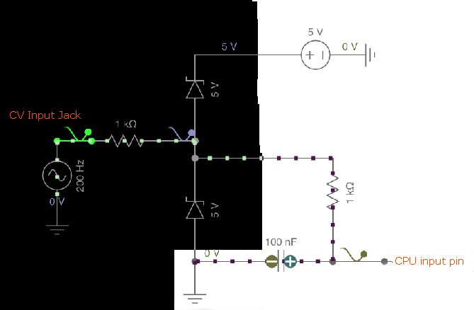
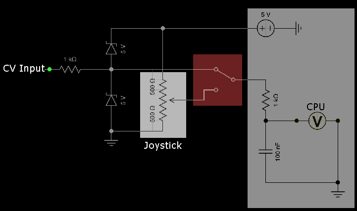
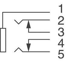
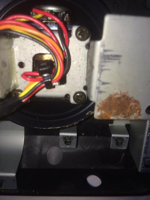
photo of the module with the important section up front. Note joystick and headphone jack:

adbe4aa6e60bda863d22cb275c90b491.png


And below is a photo of the interior of this part of my unit. From the top is the rear of the joystick assembly. Its pretty easy to remove and get to good solder points. At the bottom is the space left from removing the unneeded headphone output daughter board, and the 1/4" hole left from the headphone jack. I'll find a use or cover for it eventually. I'm intending to drill for blend pots and 1/8" jacks nearby, and connect the jack shields together and then to ground provided at the joystick unit. Or direct to chassis if I can get a good connection nearby.

5a94decf819cf637af1e33165e36f55a.png


It looks like the joystick ground goes quickly to chassis once the connector assembly reaches the main board, but with C27 0.1uf to 5v. The data entry wheel connector has an identical, separate configuration. I'm wondering if this does have implications for where I ground everything.

4f565264df9f43c59b24f93ce007606b.png
 
Last edited:
This guy **broken link removed** Band goes to input and cathode to ground. It will then clamp at a diode drop.

Max reverse voltage is non-destructive generally if the current is limited, but you really don't care about that.

5.1 V which is a standard zenier diode, but a Schotkey diode would be better. They have lower voltage drops. So, pretend that Vcc is 0V for the time being therefor eyou want the diode to conduct, so I call it follow the arrows to ground. So, the arrrow points to the +supply from the input. Using reverse logic, when the input <5V (e.g 3V) and power is 5V, the diode is reverse biased.

So, I think your missing the point, A Schotkey diode has a very low voltage drop and that's what you want to exploit. e.g. Vcc>Vcc+0.3V.

In this case,you want to pay MORE ATTENTION to the graph and not the 0.45 V absolute specification. You will be using it at MUCH lower current levels where the drop is much less.

The Schotkey diode is just a metal attached to a semiconductor.

FWIW, two Silicon diodes are sometimes used back to back to limit excursions to +- 1 diode drop.

There is also an inherent diode in the structure of the semiconductor IC (CPU if you will) but this is not robust. You will generally find specs that do tell you what the max innpput current should be.

You can clamp the positive input to say 5.1 V as well if you want. In that case, I would use a TVS diode which is designed for transients. They come in unidirectional and bidirectional versions. The unidirectional versions are used in the circuit like a Zener diode is.

BTW: There is the avalanche mechanism and Zener mechanism and both occur at about 5.1V. The diodes, though are universally called Zener though.
A Zener diode is when the breakdown voltage is actually controlled. A 400 PRV diode is a 400 V Zenier too, but there is way to much slop in the value.
 
You're right, I'm still not completely clear on how that part of the circuit works but I'm learning. My primary understanding of diodes has been as tools to chop off half a bipolar/AC wave for various reasons, and for clipping, and knowing that you have to match various kinds of diodes to different requirements. The rest has been some of the hardest for me to truly understand and retain by reading or listening to someone talk about, but I'm doing the best I can here.

What would a clamp circuit offer that the schottky pair doesn't? My understanding of clamps leads me to think they wouldn't be good here - I don't want to bias or substantially alter any input voltages until they hit overvoltage and when that happens I'd rather it just hit a hard limit and stay there. You referred to the schottky configuration as a clamp earlier, but don't clamps always use capacitors?

My circuit simulator only has zeners. I changed their breakdown voltage from 5 to 10v and tried a 0-10V signal, a bipolar 10V signal , and then threw some larger and asymmetrical bipolar voltages at it and it's still doing the job well. In fact, it hasn't breached 5V yet. I got it to put out ~500mV or so of negative voltage eventually but I'm going to assume that's a non-issue as you say. I don't expect that I can completely count on never breaching 5V with the real-life components and plugging in external devices though. So while I wanted to avoid as much signal loss as I could, my priorities here are such that when pushed, I will take an available control range of 70mV-4.75V over 0-5.1V if the latter risks frying anything. So if I just need to throw in a small voltage divider in there somewhere, maybe with a trimmer, it's a tradeoff I'm okay with at this point.
 
Last edited:
I'm dealing with the CPU not having power and having a voltage shoved down it's throat. Your not. As a side effect, the clamps I suggested would be something like -0.3 V and Vcc +0.3V give or take. With Vcc varying from 0 to 5V or so.

Here https://www.analog.com/library/analogDialogue/archives/46-02/ovp.html is an app note.

Fig 7, here https://www.analog.com/media/en/technical-documentation/application-notes/AN-402.pdf is really cool. Not exactly what you want and the bandwidth is super high.
Under fig 7, there is this :
The 1N5712 Schottky diode is used for protection from
forward biasing the substrate diode
in the AD9002 during power up transients"
I Italicized the during power up transients. You can effectively delete that fragment.
 
This guy **broken link removed** Band goes to input and cathode to ground. It will then clamp at a diode drop.

Max reverse voltage is non-destructive generally if the current is limited, but you really don't care about that.

5.1 V which is a standard zenier diode, but a Schotkey diode would be better. They have lower voltage drops. So, pretend that Vcc is 0V for the time being therefor eyou want the diode to conduct, so I call it follow the arrows to ground. So, the arrrow points to the +supply from the input. Using reverse logic, when the input <5V (e.g 3V) and power is 5V, the diode is reverse biased.

So, I think your missing the point, A Schotkey diode has a very low voltage drop and that's what you want to exploit. e.g. Vcc>Vcc+0.2V.
 
I was confused there because when I saw "clamp" my brain went to what I recently learned about clamp circuits that shift DC levels positively or negatively by using a capacitor and diode in parallel and optionally with a bias voltage. I'm sorry I'm having trouble following along. In the app note I am seeing inline diodes labelled "clamp" while I see you used it referring to a diode to ground.

I set up the circuit the way I did because of this suggestion for a very, very similar project just involving a newer microprocessor:
https://mutable-instruments.net/for...ct-them-from-negative-or-too-high-voltages/p1

So what you are suggesting is that I reverse the polarity of my diode with cathode to ground and remove the diode connected to 5V? When I try this in the simulation, it drains a 0-5V sweep to 100mV-800mV. With anode to ground, it behaves correctly as before. So 1k inline resistor and schottky to ground.. that's all I need?
 
One at a time:

A diode from the input to ground (reversed biased) won;t conduct unless the input goes negative. (that handles negative excursions)
Let me think about the positive clamp.

There is a PROBLEM with your understanding of the figure in the link.
The diodes are INSIDE the IC. They are kind of a parasitic diode.
3.3 V is the logic voltage NOT the "diode voltage or reverse bias voltage.
R1 is the actual protection.
You can gain even more protection with a Zener diode reversed biased to ground.

For the time being lets assume the CPU is Off and you apply 24 VDC. If there is a Zener clamp, the voltage gets clamped at 5 V say. But 5V still is applied to the substrate diode Without current limiting, that diode will pop. With a parallel diode to the parasitic, hopefully that will take the brunt of the overvoltage.

Note that a lot of the datasheets show an input range of -0.3 to Vcc+0.3. This is because of the parasitic diodes.

You want to add diodes externally that are more robust, but in the same configuration.

The reverse voltage should be greater than 5, I think. But like I said, the reverse voltage is non-destructive and effectively turns it into a Zener diode,
 
Last edited:
If you're referring to the mutable-instruments link, yes in that illustration the schottkys are inside the chip in the schematic, but the person in that thread who posted it was just using it as an illustration of that type of diode configuration for protection going into their device that DOESN'T have good internal protection - a nearly identical situation to mine as I understand it. I realize the 3.3V label (or 5V as the poster corrected for their project and mine) is a voltage going to to the schottky cathode, not a diode rating.

I understand and appreciate that it's often frustrating to try to help someone of my low skill level and understanding through something complicated. I've mostly only dabbled with changing/adding passive components. I do not understand logic, parasitic capacitance, substrate, etc. and while I am actively learning I can't force it. I'm just a musician hobbyist with zero formal physics or chemistry or electronics education beyond middle school trying to find my way around to make a few cool ideas happen. Maybe I need to postpone this one until I have a better grasp but I'm not giving up.

What I take from this is: 2 schottkys (the one you found on digikey), one reverse biased to ground and the other forward biased to the 5V supply, and a 5.1v zener reverse biased to ground. The schottky to ground for fast correction of negative voltages, the schottky to 5v to shut it down when power is off, and the zener to breakdown and drain overvoltage to ground? I tried this in simulation:
0bd9acbbbf24ce52ee566d9612f1ed43.png
Again both labelled 10V are intended to be schottkys. This seems to be mostly doing the job (green is input and blue is the clamped waveform -714mV-5V). But then when I change the 5v supply to 0V (power off), it's still allowing around 750mV through in both directions. That's still above the Vcc+0.3 threshhold no? I can't test this in real life with the actual unit (whose 25 year old transformer output specs might also vary a little from what is labelled) until I make and receive my parts order.

Unrelated to this issue, but I think I'll also have a voltage divider trimmer between the input resistor and before the diodes. That way I can respond to clamping when it happens and turn down the pre-clamp signal so that the control signal isn't uselessly squared off when the CPU is successfully protected from something a little too hot. Would that cause any issue with the clamping?
 
Status
Not open for further replies.

Latest threads

New Articles From Microcontroller Tips

Back
Top