Continue to Site

Welcome to our site!

Electro Tech is an online community (with over 170,000 members) who enjoy talking about and building electronic circuits, projects and gadgets. To participate you need to register. Registration is free. Click here to register now.

  • Welcome to our site! Electro Tech is an online community (with over 170,000 members) who enjoy talking about and building electronic circuits, projects and gadgets. To participate you need to register. Registration is free. Click here to register now.

transistor oscillator.. pls help me to understand

Status
Not open for further replies.

ikalogic

Member
hello,
:arrow: NOTE: i exchanged c1 and c2 with 220 uF ones to slow down the process...

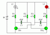
first i will explain the observation on this circuit when i realized it:

1- first led2 lights for some time and begin to fade (i gess because the capacitor C1 discharge)..
2- exactly at the moment that led2 begin fading, led1 light up, while led1 is still fading...
3- At a given moment led1 will begin fading and, at the same moment, led2 light up
1-led2 lights for some time..... [And the cycle 1-2-3 continues...]

Now, I KNOW what components decide of all the timings, this is not my problem, but i cannot figure out exaclt how it works.. and i did not find good sites to explain this, i think it is an important ussue.

2nd: while i know R2 and R3 will slow down the discharging process of the 2 capacitors, i dont know actually WHY ???, i would have understood if they were in parallel with the capacitors...am going crazy! :twisted: :evil:

thx a lot everybody[/quote]
 

Attachments

  • lights1.gif
    lights1.gif
    3.5 KB · Views: 654
This is an astable multivibrator but the gain is low, so it is oscillating in a sinusoidal manner rather than making square waves as it normally would. If R1 and R4 were larger the switching would be faster, but the LED light would be dim. A better circuit would have the LEDs driven by an emitter follower, from Q1 and Q2 collectors.
 
In your original schematic above, the reason the LEDs fade off is that the caps have to recharge through them when the other side switches on. The current path for L1 during this time is through L1, R1, C1, and the base of TR2. The path for L2 is similar. I've posted 2 possible solutions below. In the top one, D1 and D2 isolate the LEDs from the capacitors, so the LEDs turn off instantaneously. I also added D3 and D4 to protect the transistors from base-emitter breakdown, which will at best degrade beta over time, and at worst will destroy the transistors.
In the bottom schematic, The LED currents will be about 10% higher when they turn on than when they turn off, but they will turn off instantaneously. I left out the emitter diodes, because the peak reverse bias on the base-emitter junctions barely exceeds the minimum breakdown spec. I wouldn't do this in a commercial design, but you can probably get away with it in a one-off.
 

Attachments

  • lights3.GIF
    lights3.GIF
    3.9 KB · Views: 377
  • lights2.GIF
    lights2.GIF
    5.1 KB · Views: 343
ikalogic said:
hello,

Now, I KNOW what components decide of all the timings, this is not my problem, but i cannot figure out exaclt how it works.. and i did not find good sites to explain this, i think it is an important ussue.

2nd: while i know R2 and R3 will slow down the discharging process of the 2 capacitors, i dont know actually WHY ???, i would have understood if they were in parallel with the capacitors...am going crazy! :twisted: :evil:
[/quote]

The others have explained everything except your question quoted. The following explains how the timing works. Refer to the circuit below.

When T1 is on, T2 is off and vice versa. While T1 is on, C2 charges rapidly via R4, T1 B/E and D1 to the difference in potential between the 12 Volt supply and the voltage at the base of T1 (about 1.4 Volt so the difference is about 10.6 Volt). I have not shown the charging in the diagram as it is assumed to be rapid.

At the moment T2 turns on, the Collector voltage of T2 falls to about 0.9 Volt (allowing 0.7 Volt across D2 and 0.2 Volt across T2 C/E). Thus the base of T1 goes to about 0.9 - 10.6 = -9.7 Volt and so T1 is turned off.

C2 charges towards the supply voltage (+12 Volt as indicated by the dashed red line in the diagram) but when the base of T1 reaches about +1.4 Volt, T1 turns on and T2 off.

During the charge of C2, the Base voltage of T1 can be represented by the equation v = 12 +(-9.7 - 12) e^-t/tr where tr is the time constant
tr = R2 * C2. See the timing diagram.

When v reaches +1.4 Volt, t = T and so

1.4 = 12 + (-9.7 - 12) e^-T/tr

Thus 21.7 e^-T/tr = 12 - 1.4

Hence e^-T/tr = 10.8/21.7 Invert both sides gives

e^T/tr = 21.7/10.8 = 2.009

Thus T = tr ln 2.009 = 0.7 tr

But this is one half cycle. The second half cycle is approximately the same length so the period of oscillation is
2 T = 2 x 0.7 tr = 1.4 tr = 1.4 R2 C2.

Note that I have used the word charge to include both charge and discharge.
 

Attachments

  • Multivibrator_189.gif
    Multivibrator_189.gif
    4.5 KB · Views: 350
Status
Not open for further replies.

Latest threads

New Articles From Microcontroller Tips

Back
Top