Continue to Site

Welcome to our site!

Electro Tech is an online community (with over 170,000 members) who enjoy talking about and building electronic circuits, projects and gadgets. To participate you need to register. Registration is free. Click here to register now.

  • Welcome to our site! Electro Tech is an online community (with over 170,000 members) who enjoy talking about and building electronic circuits, projects and gadgets. To participate you need to register. Registration is free. Click here to register now.

Transistor Biasing

Status
Not open for further replies.

UTMonkey

Member
Dear All,

I am currently working through a useful web document on transistor biasing by Harry Lythall - **broken link removed**

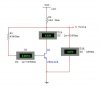
One of the early examples describes a basic biasing technique (see attached) using two resistors.

My Goal = to bias the transistor so the collector voltage equals 5 Volts with a current of 20mA.

Heres how I did it (feel free to correct)

Assumption 1= The gain of this transistor is 200 (ok I appreciate this isnt perfect in real life).

1. Ib = Collector Current (20mA) / 200 = 100uA
2. Rb = (Source Voltage - Required Collector Voltage - npn drop at base) / Ib
2a. Rb = (10V - 5V - 0.7V) / 100uA (0.0001)
2b. Rb = 43k
3. Rc = Required Collector Voltage / Required Collector Current
3a. RC = 5V / 20mA (0.020) = 250Ohms

I have tried calculations for a number of different current voltages and the calculation appear to hold up.

Here's my question (at long last!), let say I am diagnosing this diagram with just the knowledge of the resistors, voltage source, transistor and transistor gain(?) but i do not have a DMM, how could I work out the Collector Voltage and Current based only on this information?

Many thanks in advance.

Mark
 

Attachments

  • Biasing.jpg
    Biasing.jpg
    14.3 KB · Views: 341
This formula will give you the collector current. The rest should be easy:
Ic = (Vcc - Vbe) / ( Rc + (Rb/Beta))
 
Of course you can calculate the collector voltage and current. But the hFE is anywhere from 100 to 300 so your calculation will be approximate.
 
Audio, I see you are now a "Glorious beacon of light" who even outshines Nigel, who is just really nice.
:D:D:D:D:D
 
kchriste said:
Audio, I see you are now a "Glorious beacon of light" who even outshines Nigel, who is just really nice.
:D:D:D:D:D
I have a 5 green stars reputation? HEE, HEE!
What about all those noobie students that I tell them to ask their teacher?
What about all the guns-obsessed Americans that I tease?
What about all the foreigners that I ask, "No speaky zee English?"

I am surprised that I don't have 5 red stars reputation because sometimes I am not nice.
 
I've only three stars, Nigel just got his forth. Too bad they don't listen to you on Electronics-LAB duck... :)

PS I'm not allowed to critique eplanet's posts there, I don't think he likes me.
 
Everybody listens to me at Electronics-Lab except the horrible moderator who doesn't know anything about electronic circuits.
He even made up another identity for himself to agree with his false statements.

Eplanet is unusual because he is an Iranian. Arab? Muslim? Weirdo?
 
One thing still concerns me (at this stage) is the fact that as Nigel and AudioGuru still remind me is that gain varies wildly.

There are other diagrams such as the one shown that describe biasing, some quote the BC548 NPN.

According the the datasheet for this transisitor the dc gain for Vce=5V and Ic=2mA has a min gain of 110 and max of 800!!

How do you guys work with this variation? or is there anyway for you to design a circuit which utilises one aspect of the gain i.e. "I want this signal amplified by a factor of 200, and i know this is within transistor x, y and Z abilities so I will design my circuit to give me that every time"?

Or is this another one of my stupid questions?

Best Wishes

Mark
 
UTMonkey said:
How do you guys work with this variation? or is there anyway for you to design a circuit which utilises one aspect of the gain i.e. "I want this signal amplified by a factor of 200, and i know this is within transistor x, y and Z abilities so I will design my circuit to give me that every time"?

You design the circuit so it's not affected by gain variations - the circuit you posted above does this to a limited extent, due to negative feedback from collector to base. Using an emitter resistor makes it even better, adding more negative feedback - but reducing gain considerably. At sensible gains, the gain is basically dependent on the values of the collector and emitter resistors - the gain of the transistor itself obviously needs to be higher than this, but it doesn't matter how much higher.
 
Thanks Nigel, Harry Lythall's page does move on to emitter resistors which I am guessing do what you describe.

I just wanted to stop and absorb what I am reading- then moving on.

Mark
 
The datasheet for a transistor shows a curve of its base-emitter voltage at various collector currents.

Your circuit uses a transistor with a current gain of 100 to 300. Its voltage gain is not determined by the transistor's current gain, it is determined by its internal (plus external) emitter resistance and its external negative feedback.

I simulated your circuit:
1) Near max output its distortion is terrible at about 40% and its voltage gain is 100 if the source impedance is very low so that it doesn't have any AC negative feedback.
2) I added a source impedance of 2.2k ohms so that it has plenty of AC negative feedback. Then its distortion is very low and its voltage gain is reduced to 8.6.
 

Attachments

  • sim-transistor biasing.PNG
    sim-transistor biasing.PNG
    44.2 KB · Views: 205
Thanks for the screen shots and info AudioGuru but I have to admit what you have said has completely gone over my head.

Impedance?
Distortion?
40% of what? how are you measuring it?
8.6?

I understand a little of what the capacitors are for - to (de)couple the source from the circuit though to be honest at the moment i dont know why you picked that value (or the value for the output cap)?

What did the 2.2k resistor do? why that value?

I really appreciate your efforts thus far, and I don't have a problem finding this stuff out for myself... as long as you think I am on the write track in my learning.

All the best

Mark
 
UTMonkey said:
Impedance?
Your circuit has the 43k resistor providing negative feedback from the output to the input. Then its voltage gain is affected by the impedance (AC resistance) of the source that feeds it.

Distortion?
Distortion is impurity of a signal. Good audio amplifiers have a distortion of about 0.05% or less. Some opamps have a distortion that is 0.00008%. Your circuit has a distortion of about 40% so nearly half the output is impurities.

40% of what? how are you measuring it?
A distortion analyser measures a signal's amplitude then filters away its fundamental frequency then measures the remaining level of the impurities. The ratio of the impurities to its original signal is its percentage of distortion.
I use experience in looking at sine waves to judge the amount of distortion. Most people can hear 0.5% distortion and more. It sounds like the signals are buzzing and are harsh. Guitar 'fuzz" circuits manufacture high distortion amounts.

Voltage gain. The input signal has a peak voltage of 500mV (0.5V) and the output has a peak voltage of 4.3V.
4.3/0.5= 8.6.

I understand a little of what the capacitors are for - to (de)couple the source from the circuit though to be honest at the moment i dont know why you picked that value (or the value for the output cap)?
I selected the value of the capacitors to have a low reactance at the testing frequency to avoid signal loss.

What did the 2.2k resistor do? why that value?
A source impedance is usually a few k ohms. Your circuit is very much affected by the source impedance so I selected a few k ohms (2.2k).
 
Status
Not open for further replies.

Latest threads

New Articles From Microcontroller Tips

Back
Top