Continue to Site

Welcome to our site!

Electro Tech is an online community (with over 170,000 members) who enjoy talking about and building electronic circuits, projects and gadgets. To participate you need to register. Registration is free. Click here to register now.

  • Welcome to our site! Electro Tech is an online community (with over 170,000 members) who enjoy talking about and building electronic circuits, projects and gadgets. To participate you need to register. Registration is free. Click here to register now.

Switching 0-30V using a microcontroller

Status
Not open for further replies.

ekankjatwani

New Member
Hi,

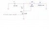
I am trying to use a 5V signal from a microcontroller to control a load switch made of an NMOS and PMOS transistor. I have attached a picture of the schematic.

The problem is that the absolute maximum rating of Vgs on most PMOS IC's that I have found is +- 20V , which I clearly exceed in this setup. I was wondering if there is a work around to this.

Also, the maximum load current expected is 200 mA.

Please let me know what y'all think.

Thank You
Ekank
 

Attachments

  • circuit.jpg
    circuit.jpg
    83.8 KB · Views: 176
Does the load have to be grounded? If not, just use an NFET and connect the load between drain and +30V. If the load must be grounded, then use a PFET with the load between drain and ground. In this case, you will need gate driver to offset the gate so it swings from 30V to ~20V to turn the PFET on. If you need help with that, write back.
 
Hi Mike,

Thank you for your response. The load has to be grounded. Can you explain the option with a gate driver and PFEt together. I have never worked with gate drivers before so I don't know a lot about them . In the mean time, i will try to find some information on gate driver.

Thanks again.

Ekank
 
hi,
You could just split the 1meg resistor into two, say top one 10K and lower one 15K, connect PMOS gate to their junction.

This would give a swing between gate and source of P type about -12V

E
 
Last edited:
Hi Eric,

That is exactly what I did at first. It seemed to work well for the most part . However, sometimes i saw the output of the mosfet would latch up and then go to its correct state on its own. I thought this might be because of the way I have the resistors placed. So i wanted to simplify the circuit and see if there is an easier way out.

I am attaching an image of the schematic in which i implemented the same idea. There is something in this circuit that is causing the mosfet to latch its output and I cant seem to understand it. So i am just trying different things.

My other guess is that there are some parisitic effects which i cant understand.

Let me know if you can think of anything that might be causing that.

THanks
Ekank
 

Attachments

  • 1.jpg
    1.jpg
    72.7 KB · Views: 177
Here is how I would do it using the parts in my junk box.

Note that the voltage divider R1 R2 constrains the voltage at the gate. With 10V of Gage drive, the PFET doesn't have to be too exotic, just handle the 30V Vds, and handle the load current.

Note that this driver is slow, so not well suited to rapid PWM, but works well as a static switch.
 

Attachments

  • DF62.jpg
    DF62.jpg
    232.7 KB · Views: 168
Also i have another question for you, why would you an NPN transistor and not NMOS ? or you could you have used either?
 
Also i have another question for you, why would you an NPN transistor and not NMOS ? or you could you have used either?

The NPN has a "threshold voltage" of Vbe or about 0.7V. In my junkbox, is hard to find an NFET that turns on well with only 5V on its gate.
 
...
My other guess is that there are some parisitic effects which i cant understand.

I looked at the datasheet. Even though it says nothing about it, I wonder if both Q1 and Q2 are on a common die substrate. If so, then there would be some wierd effects if you tied the source of Q2 to +30V while tying the source of Q1 to 0V.

If Q1 and Q2 are fabricated separately on two different substrates, then that should work fine.
 
I had the same concern as you Mike. I had read about latching issues in CMOS technologies, so I emailed fairchild about it. I haven't heard back from them yet. They use the word Complementary PowerTrench Mosfet. I read this somewhere " It is possible to design chips that are latchup-resistant, where a layer of insulating oxide (called a trench) surrounds both the NMOS and the PMOS transistors. This breaks the parasitic SCR structure between these transistors. " .

This made me think this " PowerTrench" technology of fairchild probably does the same thing forms an insulating trench surrounding NMOS and PMOS.

In the datasheet they use the term " Complementary Mosfet " to do describe this IC which to me hints towards a common substrate, but they could also be doing that because they have both NMOS and PMOS in the same package. In any case, on my design i have put two different packages for NMOS and PMOS now just to be safe.

Thank you again for your help. I will keep you posted if i here back from Fairchild.
 
I heard back from Fairchild. They do no share the same subsrtate. So i am still confused to what is causing the latch up but as i mentioned , i am going with seperate packages for NMoS and PMOs.Hopefully that fixes it.

Thank you Eric and Mike for your help.

Ekank
 
Does your input voltage range down to zero volts? If so, you are going to have a range below about 2x the gate threshold voltage that you won't be able to control. And for part of that range the mosfet will be partially on (resistive) such that you may end up letting the magic smoke out of the mosfet.

If you do indeed need to switch a voltage across the full range, you need to drive the gate from a source that is somewhat independent of the voltage being switched. You either need to pull the Pmos gate below ground, or use an Nmos part and drive the gate above Vin.

The MIC5021 from Micrel would work for the Nmos part. It uses an internal charge pump to generate a gate drive voltage above the Mosfet source pin to turn it on.

**broken link removed**
 
In the original circuit there is another "gotcha".
The leakage current (or Id @Vgs=0) of the N type in this case is 1uA. 1uA across 1M=1V, so the P gate can droop 1V typically below its Source.
According to the datasheet, Q2 (P type) has a gate threshold voltage of 1V and this can cause the P channel to start conducting when the N channel has a Vgs of zero.

I do not see how splitting the resistors with lower values as already said would not work.
 
My other guess is that there are some parisitic effects which i cant understand.
Could spurious high frequency oscillation be giving the appearence of latch-up?
 
Status
Not open for further replies.

Latest threads

Back
Top