Continue to Site

Welcome to our site!

Electro Tech is an online community (with over 170,000 members) who enjoy talking about and building electronic circuits, projects and gadgets. To participate you need to register. Registration is free. Click here to register now.

  • Welcome to our site! Electro Tech is an online community (with over 170,000 members) who enjoy talking about and building electronic circuits, projects and gadgets. To participate you need to register. Registration is free. Click here to register now.

SPI puzzle

Status
Not open for further replies.

camerart

Well-Known Member
Hi,
Can anyone comment these two examples of SPI code please, I can't see how it works? I'm mainly puzzled by the address being read/writ
Cheers, Camerart.

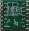
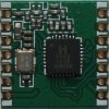
'SPI=====================================================
'Dim addr As Byte
'Dim data As Byte

'For addr = 0 To 10
'data = 200 - addr
'SPICSOn
'SPISend 0x06
'SPICSOff
'SPICSOn
'SPISend 0x02
'SPISend addr
'SPISend data
'SPICSOff
'Lcdcmdout LcdClear
'Lcdout "Write To EEPROM"
'Lcdcmdout LcdLine2Home
'Lcdout "(", #addr, ") = ", #data
'WaitMs 500
'Next addr

'For addr = 0 To 10
'SPICSOn
'SPISend 0x03
'SPISend addr
'SPIReceive data
'SPICSOff
'Lcdcmdout LcdClear
'Lcdout "Read From EEPROM"
'Lcdcmdout LcdLine2Home
'Lcdout "(", #addr, ") = ", #data
'WaitMs 500
'Next addr
 
Hi,
I am trying to read the registers on a radio chip SX1276. I have an 18F2431 connected to it via SPI.
I tried the bottom one of the examples I posted, and it read 10 values all = 0. I would expect values.
C.
 
hi C,
What is the device 'addr' of the buffer you are trying to read/write too.?
E
 
hi C,
What is the device 'addr' of the buffer you are trying to read/write too.?
E
Hi Eric,
I've been trying for weeks to crack SX1276 radio modules. The data sheet is VERY complicated! From what I can gather the registers defaults are programmed in the chip, and need changing for e,g, different frequencies etc. The chip has to be ASLEEP or STANDBY for read/write.

There is plenty of information written mainly in Arduino as NOTE these are later chips to some of the earlier stuff, and have different pin-outs. I have posted already here: https://www.electro-tech-online.com...ion-receiving-using-scr-radio-modules.149198/

C.
 
hi C,
E

'SPICSOn
'SPISend 0x06
'SPICSOff
'SPICSOn
'SPISend 0x02
'SPISend default_addr; this is the target Register
'SPISend data; data byte to write to the Register
'SPICSOff

'SPICSOn
'SPISend 0x03
'SPISend default_addr; this is the target Register
'SPIReceive data; data byte read from the Register
'SPICSOff

I don't have the time to search thru all those 5 program files, post a clip.
 
Hi Eric,
Here is part of the data sheet:
There is a second similar exploded section with more detail!

1/ What do the HEX numbers in the SPI code mean e,g, 0x06?
2/ If I only wanted to read 'say' ADDRESS 0x02, I would expect the reply to be 0x1A. What would the minimum SPI code look like?
3/ In the examples that you posted: Do I replace the default_addr with the address I am checking?
Thanks,
C.
 

Attachments

  • REG 0-16.jpg
    REG 0-16.jpg
    192.4 KB · Views: 264
hi C,
The Oshonsoft example is for a memory IC.

1/ What do the HEX numbers in the SPI code mean e,g, 0x06?
In the example from Oshonsoft, it assumes you are talking to a memory chip, 0x06 is Write Enable command. [ you do not need it]

2/ If I only wanted to read 'say' ADDRESS 0x02, I would expect the reply to be 0x1A. What would the minimum SPI code look like?
The 0x02 is a SPI Write command

3/ In the examples that you posted: Do I replace the default_addr with the address I am checking?
Yes.

This clip from my NRF TXR may explain it better:

'SPI(nRF24L01) registers(addresses)

Const wr_config = 0x20 'Config register
Const wr_en_aa = 0x21 'Enable Auto Acknowledgment
Const wr_en_rxaddr = 0x22 'Enabled RX addresses
Const wr_setup_aw = 0x23 'Setup address width
Const wr_setup_retr = 0x24 'Setup Auto. Retrans
Const wr_rf_ch = 0x25 'RF channel
Const wr_rf_setup = 0x26 'RF setup,pwr


;clip showing a Reg Write Commands
SPICSOn
SPISend wr_rf_setup '0x26 'rf setup
WaitUs 10
SPISend 0x03 '1mb data rate
SPICSOff
WaitUs 20

SPICSOn
SPISend rx_pw_p0 '0x31
WaitUs 10
SPISend dta_len
SPICSOff
WaitUs 20

'TX config
config_tx:
Disable
nrf_ce = 0
WaitMs 10
SPICSOn
SPISend wr_config '0x20
WaitUs 10
SPISend 0x36 'CONFIG as TX, CRC2, enb RX_DR ints, power dwn
SPICSOff
WaitUs 20

;clip of SPI Read from a Reg

'RX receive
receive:
SPICSOn
SPISend rd_rx_pload
WaitUs 10
For x = 0 To dta_len
SPIReceive rx_dta(x)
WaitUs 10
Next x
SPICSOff


E
 
Last edited:
hi C,
This is an example from your Table, it sets the Default RF Frequency
NOTE: if the Reg Addresses are sequential, only the first addr is required, it auto increments in Oshon

Set the CONST to suit the Used Registers

E

Const RegFrtMsb = 0x06

config_freq: ; Using default in this Example
SPICSOn
SPISend RegFrtMsb
WaitUs 10
SPISend 0x6c
WaitUs 10
SPISend 0x80
WaitUs 10
SPISend 0x00
WaitUs 10
SPICSOff
 
hi C,
The Oshonsoft example is for a memory IC.

1/ What do the HEX numbers in the SPI code mean e,g, 0x06?
In the example from Oshonsoft, it assumes you are talking to a memory chip, 0x06 is Write Enable command. [ you do not need it]

2/ If I only wanted to read 'say' ADDRESS 0x02, I would expect the reply to be 0x1A. What would the minimum SPI code look like?
The 0x02 is a SPI Write command

3/ In the examples that you posted: Do I replace the default_addr with the address I am checking?
Yes.

E

Hi Eric,
1/OK
3/OK

2/Not clear! From the Table I posted, if I only want to READ ADDRESS 0x02, the Table shows the default as 0x1A What would the minimum SPI code look like? (No writing only read) Commuting with these devices needs lots of settings, all I'm trying to do first is to confirm, I'm commuting with it.

FROM DATA SHEET: Configuration registers are accessed through the SPI interface. Registers are readable in all device mode including Sleep. However, they should be written only in Sleep and Standby modes.

I'll keep reading your examples, thanks.
C.
 
Hi

Const RegBitRateMsb = 0x02
dim data as byte

SPICSOn
SPISend RegBitRateMsb
WaitUs 10
SPIReceive data; if the Default 'data' value is still in this Reg it will return 0x1a; or what ever value you previously Wrote to RegBitRateMsb
SPICSOff


BTW: the 18F2431 has Only 8k of single Word of Instructions, take care you do not run out of program space
 
Last edited:
Hi E,
First I tried your code result '0'

Then I remembered that the chip can't be written to unless ASLEEP or STANDBY. I tried the attached code and still the reply is '0'

Const regbitratemsb = 0x02 'Address
Dim data As Byte
Const regopmode = 0x01 'Address
Dim standby As Byte
standby = 0x29

SPICSOn '////////
SPISend regopmode '/////////////
WaitUs 10 '//////////////////////
SPISend standby '////////////////

SPISend regbitratemsb '/////////////
WaitUs 10 '//////////////////////
SPISend 0x04 '////////////////
SPICSOff '///////////////////////////
WaitMs 1000 '//////////////////

SPICSOn
SPISend regbitratemsb
WaitUs 10
SPIReceive data 'If the default value is still in this reg it will Return 0x1a; Or what ever value you previously wrote
SPICSOff
Lcdcmdout LcdLine3Home
Lcdout "data= ", #data, " "


It is possible that the chip is faulty.

18F2431 point taken,

Thanks, E.
 
SPICSOn '////////
SPISend regopmode '/////////////
WaitUs 10 '//////////////////////
SPISend standby '////////////////
SPICSOff
WaitUs 10

SPICSOn

SPISend regbitratemsb '/////////////
WaitUs 10 '//////////////////////
SPISend 0x04 '////////////////
SPICSOff '///////////////////////////


EDIT:
Have you got this in the code.?
LORA_LReg = LORA_LReg OR &H80


SUB LORA.Write(LORA_LReg AS INTEGER,LORA_LData AS INTEGER) AS INTEGER
'PRINT "LORA.Write"
'PRINT "Writing ";
'PRINT LORA_RegL;
'PRINT " ";
'PRINT LORA_DataL
LORA_LReg = LORA_LReg OR &H80
PIN(LORA_PNSS) = 0
LORA_NULL = SPI(LORA_LReg) 'send register address for a read 0-&7F
LORA_NULL = SPI(LORA_LData) 'and read it in, data is returned in LORA_Reg
PIN(LORA_PNSS) = 1
END SUB
 
Last edited:
I don't have that code, because in the first instance, I'm not using LoRa, but trying the simpler OOK. (The module is transmitting at 434Mhz, so it appears to be working)

This produces '0'

Const regbitratemsb = 0x02 'Address
Dim data As Byte
Const regopmode = 0x01 'Address
Dim standby As Byte
standby = 0x29

SPICSOn '////////
SPISend regopmode '/////////////
WaitUs 10 '//////////////////////
SPISend standby '////////////////
SPICSOff
WaitUs 10

SPICSOn
SPISend regbitratemsb '/////////////
WaitUs 10 '//////////////////////
SPISend 0x04 '////////////////
SPICSOff '///////////////////////////

SPICSOn
SPISend regbitratemsb
WaitUs 10
SPIReceive data 'If the default value is still in this reg it will Return 0x1a; Or what ever value you previously wrote
SPICSOff
Lcdcmdout LcdLine3Home
Lcdout "data= ", #data, " "
 
I'll double check the connections with the oscilloscope next.

The fact that I receive '0' on the LCD, does this mean that '0' is being sent, or would it show that if nothing was working?

C.
 
Hi,
Using my old wind up oscilloscope, I couldn't get sensible readings, to prove the SPI signals are working properly. I can see flashes of app 0.3v, but it could be anything.

Eric, I think I understand SPI now, thanks for your help.

C.
 
hi C,
Please post the datasheet for the radio you are using.

Also the pin to pin connection, PIC to radio, of the SPI lines only

E
 
hi C,
Please post the datasheet for the radio you are using.

Also the pin to pin connection, PIC to radio, of the SPI lines only

E

Hi Eric,
The radio chip/module is SX1276-8, but it's long and complicated (for me anyway:eek:)

I've just seen reference to level shifting! The pic is 5v and the SX1276 is 3.3v.

Connections to follow.
C.
 
I've just seen reference to level shifting! The pic is 5v and the SX1276 is 3.3v.

Look at the 74HC125N for level shifting
 
Hi Eric,
To clarify: I use the term CHIP when I'm talking about the actual SX1276. CHIP MODULE when I'm talking about a board with a CHiP + Crystal, and a MODULE when I'm talking about a board with a CHIP +crystal + controlling Chip (Which tend to use ATMEGA).

I have CHIP MODULES: Attached

I've connected them PIC SCK to SCK--PIC SDO to MOSI--PIC SDI to MISO and PIC ???? to CS (Basically any pin on PIC??)
I may have found an error, I'll check again, and return.
C.
 

Attachments

  • SX1276 Bottom.jpg
    SX1276 Bottom.jpg
    188.4 KB · Views: 276
  • SX1276Top.jpg
    SX1276Top.jpg
    191.1 KB · Views: 267
Status
Not open for further replies.

Latest threads

New Articles From Microcontroller Tips

Back
Top