Continue to Site

Welcome to our site!

Electro Tech is an online community (with over 170,000 members) who enjoy talking about and building electronic circuits, projects and gadgets. To participate you need to register. Registration is free. Click here to register now.

  • Welcome to our site! Electro Tech is an online community (with over 170,000 members) who enjoy talking about and building electronic circuits, projects and gadgets. To participate you need to register. Registration is free. Click here to register now.

SMD pad spacing etc.??

Status
Not open for further replies.

MrDEB

Well-Known Member
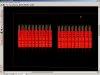
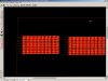
well were going forward with the 10x10 led displays.
Never worked with but don't know unless one tries.
Bought several lots of smd leds on ebay -osram lp t675 etc.
looks like the pads all need to be 2.6 x 1.5mm
should I make the pads larger-using expresspcb prg but can't find pads that size so I made pads but question if I should make the pads larger and what spacing between pads is desired??
the spec sheet shows solder mask consiberally larger than led mounting points.
need direction as wanting 2 = 10 x 10 materixs
 
I think the larger pads shown in the spec will be for heat dissipation. Smaller pads can probably be used if you dont intend to run the LEDs at their full operating current.
 
pic of planned array-work??

grid spacing is .025 traces are .012 pads are 4mm x 4mm 1mm spacing between pads
2 layer board top layer for X and bottom for Y
copper pads on under side to cover corners (no reason to etch more than needed?)
vias at each pad that needs via to connect to copper underlayer.
That hoversnap prg that was mentioned on here works GREAT!! THANKS
 

Attachments

  • Capture.jpg
    Capture.jpg
    177 KB · Views: 135
the vias are on the even # pads starting from left to right
the pic shows the center green points of the traces.
using expresspcb.
tried Eagle but to confussing-libraires, placing componets etc???
just my observation. might try some other time
 
oups made a big mistake

corrected 10 x 10 led smd pc board layout
 

Attachments

  • Capture.jpg
    Capture.jpg
    203.1 KB · Views: 185
Status
Not open for further replies.

Latest threads

Back
Top