Electro Tech is an online community (with over 170,000 members) who enjoy talking about and building electronic circuits, projects and gadgets. To participate you need to register. Registration is free. Click here to register now.
Welcome to our site! Electro Tech is an online community (with over 170,000 members) who enjoy talking about and building electronic circuits, projects and gadgets. To participate you need to register. Registration is free. Click here to register now.
1) Verification failed: the attached schematic picture does not match the binary eagle file inside the zip file.
2) To reduce board area you should use smaller parts and place them closer together.
I suppose you didn't select that name inadvertantly.
You have created a 100% power saving circuit. The MCU has power pins to be invoked (on request).
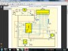
I also wonder how you managed to place components far off the two main grid sizes (0.1 and 0.05"). Some parts were not connected at all. These errors won't be indicated by the ERC, and will result in a null function PCB-design.
Last not least how did you manage to delete junction dots which are set automatically by Eagle?
The caps connected to a crystal are normally connected to ground on one side - NOTto VCC!
The Reset pin of the MCU lacks a reset connection. The way you drew it there is no way to reset the chip.
Parts without values in a schematic are a PITA. Sometimes component size depends on the value (mainly for polarized caps).
Also, add symbols for VCC and Ground (GND). They are contained in libraries "Supply1" and "Supply2". The net names will automatically be given as "VCC" and "GND", which makes routing easier when designing the board layout.
Using an ATMEL MCU it should be self explanatory to use a 6-pin programming connector (AVR-ISP-connector), which would also connect to the \RESET pin.
Finally, placing a schematic somewhere in the boondocks will lead to problems when attempting to print it. The zero reference point was in the center of your schematic. It belongs to the left hand bottom corner.
Before designing a schematic, load a frame "FRAMES" first and then place components. I shrunk the schematic size to almost DIN-A4 after it was larger than DIN-A3 initially.
Use a maximum of three different grid sizes (0.1 and 0.05 to place components and nets, and 0.025 to place labels).
This site uses cookies to help personalise content, tailor your experience and to keep you logged in if you register.
By continuing to use this site, you are consenting to our use of cookies.