Continue to Site

Welcome to our site!

Electro Tech is an online community (with over 170,000 members) who enjoy talking about and building electronic circuits, projects and gadgets. To participate you need to register. Registration is free. Click here to register now.

  • Welcome to our site! Electro Tech is an online community (with over 170,000 members) who enjoy talking about and building electronic circuits, projects and gadgets. To participate you need to register. Registration is free. Click here to register now.

Schematic critique needed.

Status
Not open for further replies.

Pommie

Well-Known Member
Most Helpful Member
As posted here, I've modified Nigel's schematic to incorporate a chip containing both the NPN and PNP transistors required. Datasheet.
This is what I came up with,
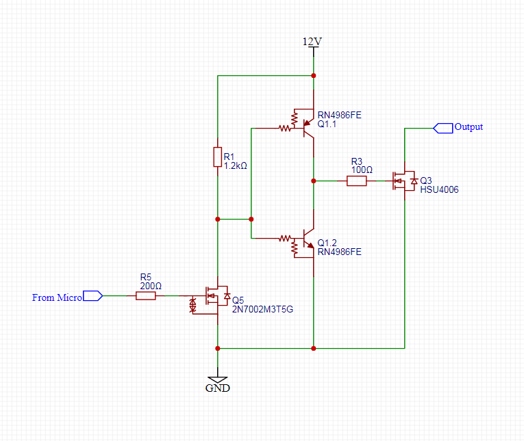
mosfet.png

The two resistors shown attached to the transistors are built in and are 4k7 base resistor and 47k emitter resistor.
Can anyone see any problems with this arrangement or have any comments?

Thanks,

Mike.
Edit, I'm assuming this will work fine with 5V or 3V logic.
 
Both transistors will turn on while the base voltage is not within a volt or so of either power rail; a high current passthrough at every transition..
 
Would switching the transistors around (so emitter followers as in Nigel's original) work? Having difficulty getting my head around this.

Thanks,

Mike.
 
Would switching the transistors around (so emitter followers as in Nigel's original) work? Having difficulty getting my head around this.

Thanks,

Mike.
Yes, basically it's a simple audio amplifier, with no bias.

I'd also like to see the 'other bits' as well, discharge resistor from gate to source, with the 10 ohm and diode in place of the 100 ohm - it's all about switching the FET ON and OFF as fast as possible.

The main problem though is probably going to be sourcing the device, components are getting quire difficult to source now, particularly 'unusual' ones.
 
I'd also like to see the 'other bits' as well, discharge resistor from gate to source, with the 10 ohm and diode in place of the 100 ohm - it's all about switching the FET ON and OFF as fast as possible.
I thought the top transistor charged the gate and the bottom one discharged it? Or did I get that wrong too?
The main problem though is probably going to be sourcing the device, components are getting quire difficult to source now, particularly 'unusual' ones.
I'm trying to pick components that JLC has "lots" of. Going to switch to a dual transistor without the resistors (C699265 - over 1300 for assembly - I only need 10). Actually, I might be better switching to individual transistors as these seem more available.

Mike.
 
2N7002 OK for 5V logic, but not 3V, Datasheets dont have any bounded
specs for 3V operation, just "typical" graphs, and some have no info on
Rdson @ Vgs low end of 3V logic drive.

A 2N3904 or like, with a base R of a K or two would suffice.

If you do use a logic level MOSFET in this position plan on a gate to
ground R of ~ 10 X the gate R, to insure MOSFET off when logic level
driver is in tri state or unpredictable when powering up to insure only
valid signals turn it on. Same for bipolar, to absorb leakage and reject
a "floating" driver condition (in tristate).


Regards, Dana.
 
I thought the top transistor charged the gate and the bottom one discharged it? Or did I get that wrong too?

For a low side switch that's right, my circuit was for a high side switch, so did the opposite - and in fact I had both low and high side examples on the same PCB. The 10 ohm charges it quickly, and the diode makes it discharge even more quickly. Even with a 10 ohm you can see the difference the diode makes on a scope.

I'm trying to pick components that JLC has "lots" of. Going to switch to a dual transistor without the resistors (C699265 - over 1300 for assembly - I only need 10). Actually, I might be better switching to individual transistors as these seem more available.

Mike.
By using seperate transistors you've got a huge variety of choices, by using a special dual transistor you're limiting your options. I use some nice little dual MOSFETS, 8 pin surface mount, P-channel and N-channel, as high current power switches - using the P-channel as the switch, and the N-channel driving it - every time I come to order them they are either out of stock, or unavailable, and I end up trying to find alternatives.
 
OK, can someone confirm if what I think is happening here is correct?
mosfet.png

When the micro pin is low, the opto is ON grounding the base of Q2 via R3 and turning Q2 on and hence the MOSFET off.
When the micro pin is high, the opto is OFF and Q1 will get a base current (~8mA) via R2 & R3, turning on Q1 and charging the MOSFETs gate to turn it on.
As the transistors have a minimum Hfe of 220 I'm assuming this will switch reasonably quickly.

And this one,
mosfet.png


This is using a P channel MOSFET and the way I "think" it works is,
When the micro pin is low, the opto is OFF, the gate is held at 12V by R2 and so the MOSFET is OFF.
When the micro pin is high, the opto is ON, the two resistors act as a voltage divider placing the gate at 10V below the source and turning the MOSFET ON.
I expect this will switch much slower than the first one but still good for on/off operations.

I'm also assuming that the opto could be replaced with an NPN but the first one would be negative logic.

Hopefully, I got some of it right.

Mike.
 
Not sure how much of a recommendation this is, but this is Siliconchip mags standard goto for MOSFET driving in their projects.

I would beef up the the drive transistors in your designs - MOSFETS can draw a substantial current in the region of several amps when turning on even if only for a fraction of a second and likewise when you have to dump the charge when turning off.
MOSFET drive.jpg
 
OK, can someone confirm if what I think is happening here is correct?
View attachment 136597
When the micro pin is low, the opto is ON grounding the base of Q2 via R3 and turning Q2 on and hence the MOSFET off.
When the micro pin is high, the opto is OFF and Q1 will get a base current (~8mA) via R2 & R3, turning on Q1 and charging the MOSFETs gate to turn it on.
As the transistors have a minimum Hfe of 220 I'm assuming this will switch reasonably quickly.

And this one,
View attachment 136600

This is using a P channel MOSFET and the way I "think" it works is,
When the micro pin is low, the opto is OFF, the gate is held at 12V by R2 and so the MOSFET is OFF.
When the micro pin is high, the opto is ON, the two resistors act as a voltage divider placing the gate at 10V below the source and turning the MOSFET ON.
I expect this will switch much slower than the first one but still good for on/off operations.

I'm also assuming that the opto could be replaced with an NPN but the first one would be negative logic.

Hopefully, I got some of it right.

Mike.
Assuming the top one is for PWM etc.?, than I'd still like a diode across R4 :D which will help reduce heat in the MOSFET by turning it OFF faster.
 
Here's a beefed up version,
mosfet.png

The transistors can handle 3A each. The opto transistor can handle 50mA hence the 240Ω resistors. The two 22Ω resistors are to handle the high current and wattage. All need to be SMD so the resistors are 1206 to handle the current. The wattage on each of those 22Ω resistors is 12²/22=6.5W, though only for a very short time(??). Base current is minimum 25mA and with Hfe of 220 it should switch pretty fast.

Silly thing is this is going to switch very slowly (~10Hz) but I thought if I could get a good design in readily available parts then why not. It's going to control a heater using PWM, I'm thinking 1 to 100mS to represent 1 to 100% hence 10Hz.

Mike.
 
Do I still need a diode to turn it off faster or will 11Ω do it?

Mike.
I used a 10 ohm resistor, and adding the diode speeded it up, and made it run cooler.

I see no reason for bigger transistors, bear in mind any current pulse is extremely short, so not of any concern. My original design used BC327/BC337 (as in the SiliconChip example above) - however the BC327 wasn't available!!!, and I substituted a BC557 instead, a lower power device. It works perfectly fine, and turns the FET on and off pretty quickly - my PWM is running at 124KHz or so, the fastest I can get while still keeping 8 bit resolution, keeping 10 bits would have been nice, but there's no need, and I'd sooner have the faster speed.
 
Here's a beefed up version,
You would definitely need a different opto isolator with the much lower load resistor - it would have been marginal with the original 1.2K but that is way out of spec; it's a 50% CTR device.
 
You would definitely need a different opto isolator with the much lower load resistor - it would have been marginal with the original 1.2K but that is way out of spec; it's a 50% CTR device.
I don't understand. The transistor in the opto can have a collector current of 50mA, a 240Ω resistor limits 12V to 50mA.
Or, are you saying that if the LED current is only 20mA then the transistor collector current will only be 10mA and result in the opto overheating?

Mike.
 
Or, are you saying that if the LED current is only 20mA then the transistor collector current will only be 10mA and result in the opto overheating?
Exactly - it's got a CTR of 50% so no more than 25mA through the transistor with 50mA [absolute max] LED current.

That's worst-case, but you need to design to allow for components at the limits of data sheet specs, to guarantee everything works as it should.

If you use an opto with eg. 300% CTR, 20mA LED current should be fine.
Or add another transistor stage to handle the low value load resistor and keep the opto current requirement down?
 
I've ditched the opto and used a BC848B instead, figure it'll saturate at a base current >10mA. Main problem is trying to find items that are available.

Mike.
 
Status
Not open for further replies.

Latest threads

New Articles From Microcontroller Tips

Back
Top