Continue to Site

Welcome to our site!

Electro Tech is an online community (with over 170,000 members) who enjoy talking about and building electronic circuits, projects and gadgets. To participate you need to register. Registration is free. Click here to register now.

  • Welcome to our site! Electro Tech is an online community (with over 170,000 members) who enjoy talking about and building electronic circuits, projects and gadgets. To participate you need to register. Registration is free. Click here to register now.

Questions for my schematic on Eagle

Status
Not open for further replies.

whiz115

Member
Hi!

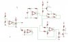
i need help for the following schematic...

1) where's my op-amp pin #4 and #11? why i can't find it?

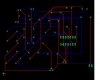
2) Is there any special way i should arrange my components on
the PCB? it's a mess!!!

3) How can i make my PCB only one layer? (no bottom side)

4) Some components aren't connected, should i use more junctions?

5) I'm building my schematic in a limited space! (half page) is it limitation
of the free version of Eagle or i'm doing something wrong?

thank you! :)


P.S it's not totaly finished yet...
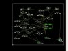
 

Attachments

  • mysch.jpg
    mysch.jpg
    43.8 KB · Views: 443
  • mypcb.jpg
    mypcb.jpg
    43.6 KB · Views: 233
  • mypcb1.jpg
    mypcb1.jpg
    23.5 KB · Views: 288
Last edited:
as for the pin 4 and 11 , eagle is neglected them as they are the vcc and gnd .

i recommend something else to you , you can instead of adding this opamp from the library ....better to add a full ic package with 8 pin or 20 pin or what you need.

go to ic pagakge in the library and add your required layout ..... it will be so easy to work with this .

i know how to solve your current problem and to show he 11 and 4 pin but it's not easy and sometimes problems occured.

you asked how to make a single layout and to stop the top one :

go to the DRC button at the toolbar and in the dialogue you have to specify your wire distance and tolelarnce and other specifications.

after that close it and go to the button AUTO ,in the dialogue , you will find TOP and Bottom , open the top scrollbar and select NONE , then it will never do top layer again ,

ask me if you have further problems

and try to nest your component places , do not put and leave like that .

FARAG
 
On the schematic editor toolbar you will find the INVOKE button just above the "T" or text button. Select INVOKE then click on any of the op-amps and Eagle will show the missing pins which you are allowed to place.

It is common to place them on one of the the op-amp symbols or in the area where you have specified bypass caps etc.

Unless you are doing surface mount parts it is the TOP layer you want to not use for SS boards. When the route tool is active there is a layer indicator in the upper left side of the screen. It allows you to choose RED for top and BLUE for the bottom layer. If you keep it blue it will always create you traces on the bottom.

Avoid the autorouter till you get some experience.
 
Thank you guys! your advices are really helpful! :)


3v0 said:
Avoid the autorouter till you get some experience.

if i avoid autorouter how am i going to create my PCB rails?! :confused:


I did what watzmann proposed and although it shows only the button (blue rails) autorouter has hard time to create them! probably it's my messy aligment of the components right? :D

also i want to know how i invert the pins of the op-amp so i can have Pin #3 in place of Pin #2?
 
3v0 said:
You seem to be missing basic concepts that are too numerous to teach you here.

You need to work through a tutorial or too.


it is obvious that i'm missing everything! i don't have the slightest idea on how to work on Eagle...so how i invert the pins of the op-amp so i can have Pin #3 in place of Pin #2?

the idea not to use a full ic package and use the op-amp symbol i got it from a tutorial :D
 
Use the mirror tool. It is just below move and above group.

It will mirror the part for you. You may have to flip it around again to get it back into position.

If you want to move pins around that you can not do by mirror and flipping/rotate then you need to make a custom part.
 
so how i invert the pins of the op-amp so i can have Pin #3 in place of Pin #2?
If you do that, then the circuit won't work. :confused:
 
kchriste said:
If you do that, then the circuit won't work. :confused:
We were talking about the schematic. As long as the numbers stay the same the actual position/location on the symbol does not matter.

My poor choice of words may have been the problem
me said:
It will mirror the part for you.
If you use the mirro tool in the board/layout editor it will move the part to the other side of the board. The traces are re-routed so they go to the correct pins but design rules are not followed.
 
Last edited:
If you do that, then the circuit won't work.
why? just because it helps me if i have the minus (-) up and the plus (+) down?
Oh ok. I thought you were talking board layout, not schematic. When placing or moving the part on the schematic, just right click twice to rotate the part 180 degrees and then click the center mouse button to flip it. Voila! + & - pins will be swapped.
 
kchriste said:
Oh ok. I thought you were talking board layout, not schematic. When placing or moving the part on the schematic, just right click twice to rotate the part 180 degrees and then click the center mouse button to flip it. Voila! + & - pins will be swapped.

that's EXACTLY what i was asking!!! :D i didn't made it clear? :rolleyes:

so here i come with another question... can i pass my schematic to a spice program like LTSPICE so i can check my circuit or Eagle has it's own spice program?

also i still got problems with my pcb layout because autorouter can't calculate all the rails...
are there any advices or tutorials on how i can arrange my components on the pcb?
 
Last edited:
whiz115 said:
also i still got problems with my pcb layout because autorouter can't calculate all the rails...
are there any advices or tutorials on how i can arrange my components on the pcb?

Look at how the parts relate to each other. Connectioned parts should be placed next to each other when possible. You can see how connected parts are by the number of air-wires between them. Move the parts around and flip them till you get the best fit (fewest crossed wires, shorted traces etc).

I start out with a fairly loose/open/sparse layout.

After all the air-wires have been routed (by me, not the brain dead auto router) I use the move tool to close the spaces.

Next I use the DRC tool to check clearances.

A PCB is like a painting but with electrical and physical restraints. I like to layout a board then walk away from it for a while. When I return to it I can see things to change, or how to fix nagging problems. I may do this several times over a few days.

I so not know of any connection between Eagle and spice.
 
whiz115 said:
mirror makes the left right and the right left... :p
it doesn't make it upside down...

With the board layout:
Rotate will do that. Mirror WILL move the part to the other side of the board (change its layer). Try it with a smt component and you will see. It only appears to swap the left and right because your perspective of the board does not change with the part.

I find that the easiest way to start routing is to make a fat power bus on either side of the PCB, then start routing the power and ground connections to the parts, then the decoupling caps (if any). That way I don't end up with long or complicated power rails.
 
Last edited:
Just to make things clear.

When talking about mirror it is important to specify if you are talking about the schematic or the board.

In the schematic mirror reflects the symbol along an axis.

With the board mirror moves the part to the other side/layer.(top->bottom or bottom->top)
Works with any component not just smd parts.

The OP was talking about the pins on a symbol but the thread may have drifted.
 
Last edited:
Status
Not open for further replies.

Latest threads

New Articles From Microcontroller Tips

Back
Top