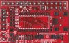
1) The picture on the left has red silkscreen right?
So the layer that is bright red, what layer would that be in Eagle.
and the layer that is dark red, what layer would that be in eagle.
2) Also the pads, the silver things, is that solder? or is that something else.
I understand that you could manually place solder paste onto the pads
but if this is a bare pcb,
3)what material is that? Is it copper? gray copper? lol
4) I can see on the left picture, name layer, there is an exclamation mark, which has the exclaimation mark cover two vias at least. Would that cause the vias to be non conductive at all?
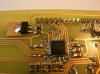
5) The picture on the right, which has the soldered vias, the soldered joints are huge, which makes me believe the vias must be big as well. hmmm.
I mean hes done a good job for a double layer board with vias. But anyone knows where he could have improved?
Look forward to your guys responses.
Thanks,
Ben
So the layer that is bright red, what layer would that be in Eagle.
and the layer that is dark red, what layer would that be in eagle.
2) Also the pads, the silver things, is that solder? or is that something else.
I understand that you could manually place solder paste onto the pads
but if this is a bare pcb,
3)what material is that? Is it copper? gray copper? lol
4) I can see on the left picture, name layer, there is an exclamation mark, which has the exclaimation mark cover two vias at least. Would that cause the vias to be non conductive at all?
5) The picture on the right, which has the soldered vias, the soldered joints are huge, which makes me believe the vias must be big as well. hmmm.
I mean hes done a good job for a double layer board with vias. But anyone knows where he could have improved?
Look forward to your guys responses.
Thanks,
Ben
Attachments
Last edited:
