Speakerguy
Active Member
I am working on a board right now and I have a question.
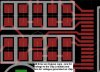
In the attached image there are 3 bypass capacitors for an IC. The leftmost is circled in yellow, and the other two are immediately to its right. The cap in the middle of the trio is the bypass cap for power to the chip; the other two caps are external bypass caps for voltages developed on the chip itself.
The cap circled in yellow is a small bypass cap (220nF) for one of the on-chip generated voltages (compensation cap for an internal regulator). I 'split' its pads with a trace for the power supply to the chip.
Is this generally an OK practice, or do I need to worry about running traces under components like that? Is that a no-no? These will be professionally made boards so I won't have any problems etching or anything like that. I'm more interested in potential problems with signal coupling, EMI, stuff like that.
Thanks for any help.
") ). But it is very nice to know that kind of information. I would like to become something of a layout expert, so I appreciate knowing those kinds of things.
). But it is very nice to know that kind of information. I would like to become something of a layout expert, so I appreciate knowing those kinds of things.