Triode
Well-Known Member
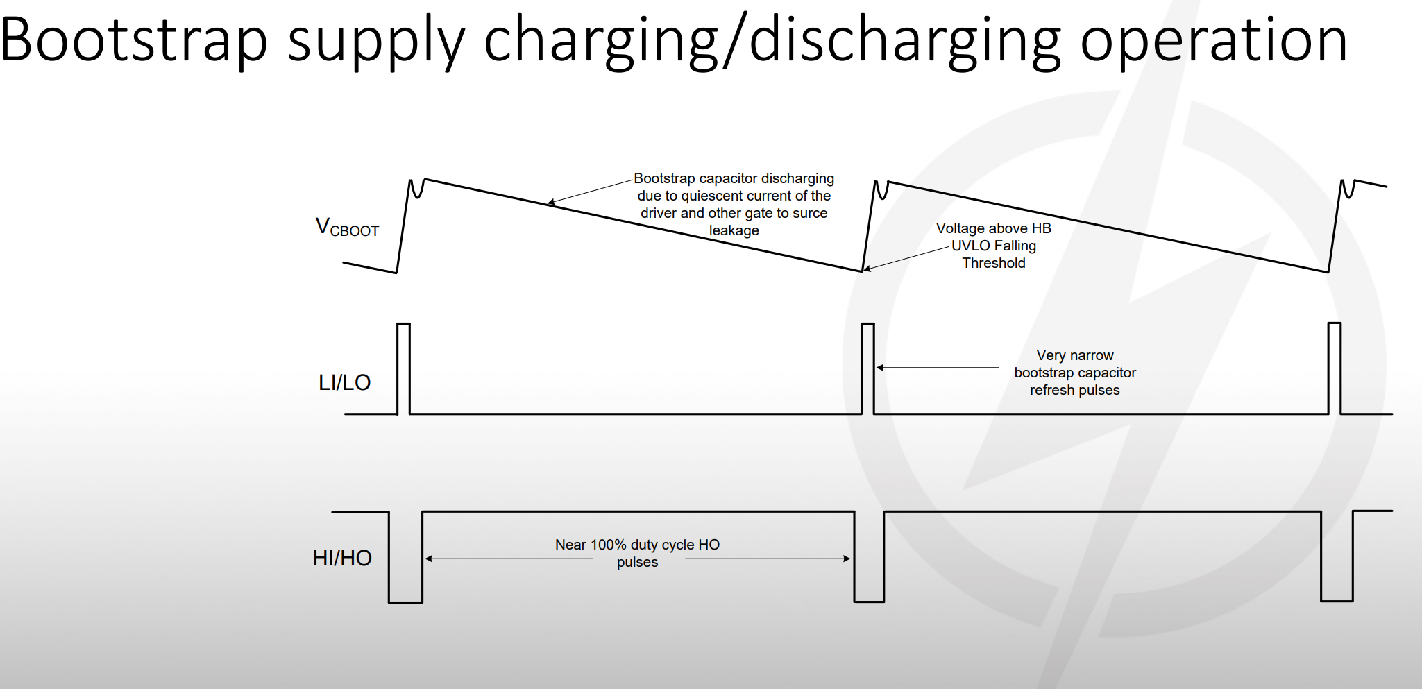
So I've been using a lot of these training documents from TI and others to learn design because really they seem more practical than most text books. I had a question about part of this document. I've been trying to get better at designing motor drivers. In this case for BLDC but it could apply to every half bridge based design.
I'm confused about this part

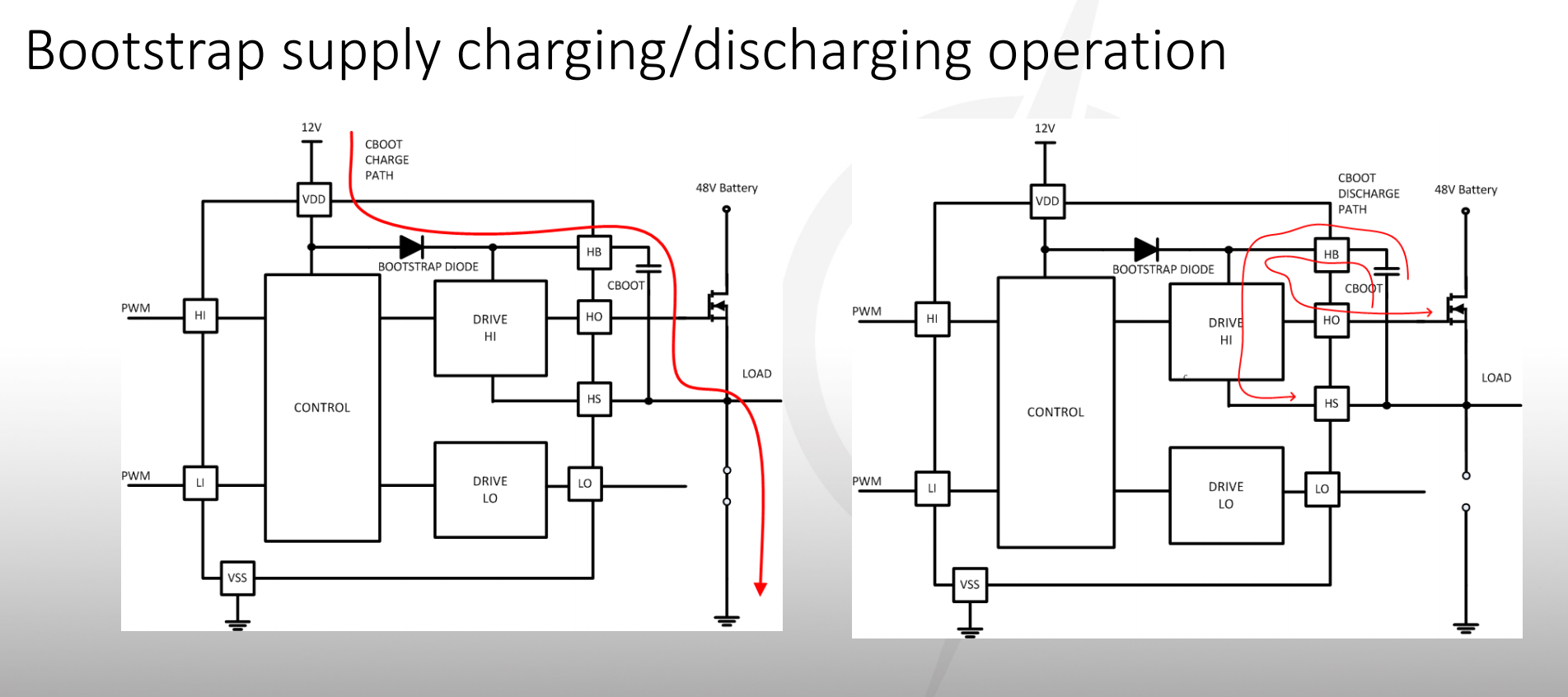
for easier reference here is the circuit under consideration

Is this just reinforcing the point that you can't go 100% duty cycle, and that you must recharge the bootstrap periodically? Is there some way to calculate how frequently or how long this must be done, or do you usually just tune it experimentally by scoping the gate pin and watching for the voltage to drop too close to below saturation? I see the equations on page 8, and I can find the drain to source leakage current on the datasheet. But I'm not sure about gathering all of the quantities used in those equations other than experimentally.
Also, about that little dip at the top of the ramp for Voltage of Cboot. I get that it would drop rapidly while initially charging the mosfet gate. But why is it parabolic and recovers? There is no energy coming in anymore from the Cboot charge path that I notice, seems like it would drop sharply till the gate is charged then falloff slowly from quiescent current and gate source leakage, I don't see why it goes back up.
Thanks!
I'm confused about this part
for easier reference here is the circuit under consideration
Is this just reinforcing the point that you can't go 100% duty cycle, and that you must recharge the bootstrap periodically? Is there some way to calculate how frequently or how long this must be done, or do you usually just tune it experimentally by scoping the gate pin and watching for the voltage to drop too close to below saturation? I see the equations on page 8, and I can find the drain to source leakage current on the datasheet. But I'm not sure about gathering all of the quantities used in those equations other than experimentally.
Also, about that little dip at the top of the ramp for Voltage of Cboot. I get that it would drop rapidly while initially charging the mosfet gate. But why is it parabolic and recovers? There is no energy coming in anymore from the Cboot charge path that I notice, seems like it would drop sharply till the gate is charged then falloff slowly from quiescent current and gate source leakage, I don't see why it goes back up.
Thanks!
Last edited:
