Continue to Site

Welcome to our site!

Electro Tech is an online community (with over 170,000 members) who enjoy talking about and building electronic circuits, projects and gadgets. To participate you need to register. Registration is free. Click here to register now.

  • Welcome to our site! Electro Tech is an online community (with over 170,000 members) who enjoy talking about and building electronic circuits, projects and gadgets. To participate you need to register. Registration is free. Click here to register now.

question about flyback diode

Status
Not open for further replies.

nrebol

New Member
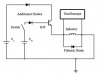
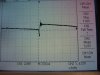
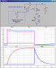
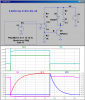
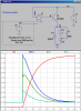
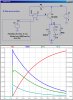
hi, i am a physics student and i am building a circuit to connect to a very large inductor used in a Magneto-Optical trap. Basically she wants to eliminate the voltage spike resulting from turning off the power to the inductor, so she had me test some diodes in a flyback circuit. (i attached the circuit diagram). the problem is the diodes don't actually reduce the spike to a decent level. In fact, the BJT in the circuit does the most to reduce the spike. Also, i occasionally get a oscillation in the voltage as shown in the other image attachment. Neither myself nor my professor can explain why the oscillation occurs.


anyone's help would be greatly appreciated, thanks in advance
 

Attachments

  • realcircuit.jpg
    realcircuit.jpg
    56.4 KB · Views: 632
  • bat_bjt_diode.JPG
    bat_bjt_diode.JPG
    908.1 KB · Views: 353
What is the current and voltage of the inductor? What are the supply voltages? What is the diode rating?

With the circuit in the thumbnail, the inductor voltage should drop to about -0.7V when the transistor is turned off, since at that point all the inductor current should be flowing through the diode. If that is not what you see than the circuit must not be wired as shown.

Also, I don't understand your comment that the BJT does the most to reduce the spike.

I don't see any purpose for the additional diodes.

Oscillations are likely due to stray capacitances and inductances in the circuit. A small RC snubber circuit (say 30Ω in series with 0.1µf) across the inductor may help suppress them.
 
sorry, i forgot to add that information:


the supply voltages were 9.0 V for the V_c and 8.1 for V_b.

The voltage through the inductor was 7.13 V, it has an inductance of 5.64H and a resistance of 4ohms.

the diode i used was had a forward current of 1A, forward drop voltage of .67V and peak forward current of 75A. (**broken link removed**)

as for the BJT, there is a bit of a delay when the current is stopped through it. like if there was a switch before the Base of the BJT. so the forward current goes to zero not quite as quickly. or at least that is my guess as to what was happening. when i didn't have the bjt in place and just had a power supply to connected to the inductor, the spikes i got were almost twice as big as when it was connected (~12V as opposed to >20V). When the flyback diode was in place with the BJT, the spikes were only a few volts less in size than that(~10V). But with out the BJT and with the flyback diode, the spikes were still at around 10-11V.


thanks for the help!
 
Are you aware that it takes about 8 SECONDS to establish the current in the coil, and another 4 sec for the current to cease after the transistor is turned off! Look at the attached simulation: I modeled a switch in the base circuit that turns on at 1s, is on for 8s, and then turns off. I had to add a resistor to limit the base current (I hope you are using one, otherwise you will likely blow up the transistor). Note that when the transistor shuts off, the inductor current continues to flow through the snubber diode. The energy stored in the inductor is dissipated in its own coil resistance (4Ω). Note that the snubber diode clamps the reverse voltage across the inductor at about -0.5V with respect to ground.

This is not a very good way of driving the inductor, because of the power lost in the transistor which when connected in the common-collector configuration can not turn on fully. The power dissipation in the transistor is over 2W, and would have to be mounted on a heatsink.

Contrast that to the common-emitter configuration which is shown in the second circuit. Note that the snubber still provides a current path for the coil current after the transistor turns off, this time clamping the voltage ~ 0.5V above the 9V supply voltage while the coil energy is dissipated. The power dissipation while the transistor is turned on in this configuration is much lower; about 1/2W.
 

Attachments

  • Df12.png
    Df12.png
    34.8 KB · Views: 306
  • Df13.png
    Df13.png
    42.1 KB · Views: 354
Are you aware that it takes about 8 SECONDS to establish the current in the coil, and another 4 sec for the current to cease after the transistor is turned off! Look at the attached simulation: I modeled a switch in the base circuit that turns on at 1s, is on for 8s, and then turns off. I had to add a resistor to limit the base current (I hope you are using one, otherwise you will likely blow up the transistor). Note that when the transistor shuts off, the inductor current continues to flow through the snubber diode. The energy stored in the inductor is dissipated in its own coil resistance (4Ω). Note that the snubber diode clamps the reverse voltage across the inductor at about -0.5V with respect to ground.
since his SCOPE trace is showing a 25uS fall time and an inconsequential rise time I suspect he is looking at millihenries or microhenries.
 
since his SCOPE trace is showing a 25uS fall time and an inconsequential rise time I suspect he is looking at millihenries or microhenries.
Those times are due to stray capacitance and the speed of the transistor, which determines the voltage risetime and falltime, not the inductance of the inductor. That inductance determines the current risetime and has no effect on the voltage risetime.
 
Those times are due to stray capacitance and the speed of the transistor, which determines the voltage risetime and falltime, not the inductance of the inductor. That inductance determines the current risetime and has no effect on the voltage risetime.

i was looking at voltage and thinking current ... there is no way, however that the inductance value could be in henries since that would have the voltage a square wave between the power rail and the -0.6V diode drop. of course the spike in the circuit given would likely blow past the diodes destroying the switch transistor.
 
Are you aware that it takes about 8 SECONDS to establish the current in the coil, and another 4 sec for the current to cease after the transistor is turned off! Look at the attached simulation: I modeled a switch in the base circuit that turns on at 1s, is on for 8s, and then turns off. I had to add a resistor to limit the base current (I hope you are using one, otherwise you will likely blow up the transistor). Note that when the transistor shuts off, the inductor current continues to flow through the snubber diode. The energy stored in the inductor is dissipated in its own coil resistance (4Ω). Note that the snubber diode clamps the reverse voltage across the inductor at about -0.5V with respect to ground.

This is not a very good way of driving the inductor, because of the power lost in the transistor which when connected in the common-collector configuration can not turn on fully. The power dissipation in the transistor is over 2W, and would have to be mounted on a heatsink.

Contrast that to the common-emitter configuration which is shown in the second circuit. Note that the snubber still provides a current path for the coil current after the transistor turns off, this time clamping the voltage ~ 0.5V above the 9V supply voltage while the coil energy is dissipated. The power dissipation while the transistor is turned on in this configuration is much lower; about 1/2W.
I agree that the CE configuration is generally a better way to drive the coil.
That being said, why did you need a series base resistor in the CC configuration? Base current should be limited to Ie/(β+1) in the absence of a base resistor.
 
i was looking at voltage and thinking current ... there is no way, however that the inductance value could be in henries since that would have the voltage a square wave between the power rail and the -0.6V diode drop. of course the spike in the circuit given would likely blow past the diodes destroying the switch transistor.
Which is why I said his circuit measurements do not correspond to the oscilloscope pictures.

As to the voltage spike, it should be no more than -0.7V as long as the diode can carry 2A maximum for the 4 seconds it takes the current to decay to zero. The Op's 1A diode may be a little marginal for that.
seems he needs to take the measurements again, and record all the component numbers as well
 
I agree that the CE configuration is generally a better way to drive the coil.
That being said, why did you need a series base resistor in the CC configuration? Base current should be limited to Ie/(β+1) in the absence of a base resistor.

I resimed it without a base resistor. I added a WAG at stray capacitance on the emitter of the transistor. Since the deflection coil is huge, 400pF of stray is likely low. Note that when the switch closes, the emitter cannot instantaneously follow, causing almost 3A of base current until the emitter catches up to the base. Putting in the base resistance reduces the peak base current to ~650mA. Adding the resistor limits the peak current but slows the rise time.
 

Attachments

  • DF12a.png
    DF12a.png
    38.4 KB · Views: 174
  • DF12b.png
    DF12b.png
    40.3 KB · Views: 168
Last edited:
Base current risetime is on the order of a few picoseconds, which may not be realistic. This creates high C*dv/dt currents. The resistor is probably a good idea, at least for the simulation. I ran the sim with two 3055 models which were apparently different from yours, and got much higher peak base currents - 90 Amps on one, can't remember the other one.

BTW, TIP3055 and 2N3055 list max base current as 7 Amps.
 
Status
Not open for further replies.

Latest threads

New Articles From Microcontroller Tips

Back
Top