Continue to Site

Welcome to our site!

Electro Tech is an online community (with over 170,000 members) who enjoy talking about and building electronic circuits, projects and gadgets. To participate you need to register. Registration is free. Click here to register now.

  • Welcome to our site! Electro Tech is an online community (with over 170,000 members) who enjoy talking about and building electronic circuits, projects and gadgets. To participate you need to register. Registration is free. Click here to register now.

question about designing a evaluation board

Status
Not open for further replies.

Chengjun Li

New Member
I have a question about a schematic of evaluation board provided by a company.

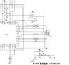
The lower right corner of the schematic below shows a simple circuit for the power supply section of the evaluation board. It seems that there are two ground, one is GND and the other is FG, there can be connected together through a jumper. The components on the board are connected to GND rather than FG.

This kind of design made me confused.
I think in this case, most area of board(copper pour) will be FG, GND only exists in several traces, am I correct? If I am correct, then what's the benefit of doing this?
 

Attachments

  • schematic.jpg
    schematic.jpg
    62.6 KB · Views: 144
  • PCB (1).jpg
    PCB (1).jpg
    12 KB · Views: 126
Last edited:
I cannot log on to that site without joining?
GND is the Chassis or circuit common, FG is the Earth ground.
Some favour circuit isolation, it seems that they offer the alternative option of connecting Common to earth.
This is often done for noise prevention and/or safety.
They should show different symbols for each.
Max.
 

Attachments

  • GNDsymb copy.jpg
    GNDsymb copy.jpg
    23.3 KB · Views: 116
  • GroundObjects.jpg
    GroundObjects.jpg
    63.9 KB · Views: 115
I cannot log on to that site without joining?
GND is the Chassis or circuit common, FG is the Earth ground.
Some favour circuit isolation, it seems that they offer the alternative option of connecting Common to earth.
This is often done for noise prevention and/or safety.
They should show different symbols for each.
Max.

Sorry, I've revised the threat by uploading the pictures.
I think you are right, but I still feel confused, if connecting common to ground can prevent noise and is safe, why didn't the board designer directly connect these two ground rather than placing a jumper? Is there any bad points of connecting these two?
Also would you please help me check whether what I said in the threat is right? I want to make sure when I design the PCB, I have to route GNDs one by one rather than pour a ground plane, because in this case the ground plane will be FG rather than GND.
 
What is the exact function of the board?
Generally if the power supply to the board is isolated, i.e battery or mains supply that is galvanically isolated, then if this design is not stand alone but integrating with other systems there can be an advantage to earth grounding, it all depends on what type of external influences there may be on the board such as interfacing with noise creating circuits.
If a stand alone application then there is probably no need to earth ground, but this does not affect the ground plane which is usually the supply common or GND.
The board function is one main criteria.
Max.
This board is used to accurately measure extremely small capacitance difference between two capacitors. I only need to connect the external capacitors to the connectors of the board, the output is the capacitance difference.

So I am wrong, I don't need to connect GND from different components one by one, I can still pour copper on top and bottom layer of the board and defined it as GND?
 
GND is the system, or circuit, or signal ground, the reference potential for all of the circuit's operational voltages. FG is Field Ground, an industrial control term for Earth Ground. This is not necessary for proper circuit operation. Connecting the two brings the system ground down to 0 V difference from Earth. Without that connection the two could be tens or hundreds of volts apart. This usually is not a problem with a stand-alone device, but if you connect to other devices for input or output signals, it is best if everyone agrees on what "ground" is. In systems with sensitive signals, this sometimes can cause problems with ground loops inducing noise, which is why the connection is optional.

ak
 
My understanding is FG is Frame Ground or Chassis Ground or eventually Earth.

The thing to remember is that in the ideal case all grounds go to a single point. Ideal, unfortunately, can't happen, so you do the next best thing,

You keep them separated depending on their function and join them "at one place".

Signal ground is effectively a reference where no or very little current flows. The power supply ground has lots of current bursts on them. We can also have "digital ground" which can be more dirty than other ground points.

Finally, we have the chassis ground which shields everything.

Eventually, we tie all of these together at one point. The "one point" is harder to visualize when other stuff gets connected.
e.g. consumer audio amplifiers.

Ideal would mean differential transmission with a transmission line characteristics. e.g. 110 ohm twisted pair driven differentially.

I will add yet another concept called guard. This is a driven source of the same potential. Triax cables have two shields and an inner conductor. The inner shield is usually driven at the potential of the inner conductor. The outer conductor is earth.
This can prevent leakages in the pA and fA (femto-amp) region.
 
Status
Not open for further replies.

Latest threads

New Articles From Microcontroller Tips

Back
Top