Continue to Site

Welcome to our site!

Electro Tech is an online community (with over 170,000 members) who enjoy talking about and building electronic circuits, projects and gadgets. To participate you need to register. Registration is free. Click here to register now.

  • Welcome to our site! Electro Tech is an online community (with over 170,000 members) who enjoy talking about and building electronic circuits, projects and gadgets. To participate you need to register. Registration is free. Click here to register now.

Problem With Ringing on Gate

Status
Not open for further replies.

clw

New Member
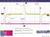
Attached are waveforms of the Top FET drain-source voltage and Top FET gate-source in one phase of a 3-phase motor drive. I am trying to diagnose a 2V (or so) ring on the FET's gate signal. I'm currently running with a vbus across the bridge of 60V. The load is light - resistive, but with unknown amount of inductance since I'm using wire-wound resistors. The load R's are connected VBUS+ to OUT and VBUS- to OUT.

The ringing on the upper FET's gate occurs coincident with the turn-on of the lower FET. Conversely - I see similar ringing on the lower FET's gate when the upper FET turns on.

I do not know if this ringing should be of concern. Ultimately I'll be at VBUS = 300V and switching multiple Amps. Currently at 60V and sub-amps. I've tried slowing down the turn-on by increasing the gate R to 100 ohm. The gate rise time changes from about 700nS to about 5uS - FET turn-on time changes from about 120nS to over 1uS, but -the ringing is unchanged.

The FETs are N-channel STY80NM60 and the gate drivers are Avago ACPL333J.

Any ideas?
 

Attachments

  • Gate Ringing.JPG
    Gate Ringing.JPG
    77 KB · Views: 597
Last edited:
Please attach your schematic.
Usually a low-value resistor is in series with the gate pin mounted directly at the gate pin. This prevents oscillation and ringing.
Supply bypass capacitors are also important.
 
One power phase section schematic attached. As mentioned in the initial post - I do have gate resistors - they are located several mm from the FETs. The drivers are also very close. All drain and source switch and power nodes are buried power planes (multiple) designed to carry high currents.
 
Last edited:
Your circuit has a layout problem. The 10 ohm resistors in series with the gates must be directly at the gate pins, not several mm away.
 
The datasheet may have some information about this issue on pg 22 where it discusses calculating the value of the pulldown. That 2V ringing is about three diode drops and the load is definately capacitive. Perhaps the values of your R39 & 43 need to be reduced to ensure the Output current does not approach zero as described in the datasheet.
 
I should have mentioned that the waveforms presented were with R39 and R43 already changed to 1K ohm - no change. The ringing is not present at vbus = 0V. It grows to approx 2V at vbus = 60 (the limit of my bench supply).

In reply to audioguru - I find it hard to believe that the gate R must be less than several (I measure 6) millimeters from the FET gate leg pad. The legs on the FET are longer than that!. I will do an experiment where I lift the avago output pin and connect directly to the fet's gate via a gate R - thus eliminating the turn-off gate resistor traces and the avago's vclamp circuit.

As soon as I get some non-inductive load resistors I will try those as well.
 
The ringing could be coupled from the output power into the scope return line ('ground clip').
 
I was wondering about that. Something I just noticed is that a second probe connected to the scope picks up the ringing (identical shape, similar amplitude, but 180 degrees out of phase) just sitting on the static mat.
 
Ringing is easily induced in the ground of an oscilloscope. I have had high speed digital circuits where I connect the probe right to the ground lead on the circuit and can see transient ringing due to switching in the circuit. Incidentally that's a good check to determine whether any of the ringing you see is ground induced. Just connect the scope probe to the ground lead when connected to the circuit ground.

To minimize this, use as short a ground lead as possible from the scope probe and connect the ground as close as possible to a ground near the point being measured. Also don't have any other ground connections to the scope.
 
In this case the ground node is the upper mosfet's source which is the half-bridge switching node. Do I have any chance of making a clean measurement with this node as the ground reference on a single ended probe? Should I be using a differential probe? I have tried using two single ended probes and the scope to subtract the waveforms, but I still see the ringing. The ground leads on my probes are about 5" long
 
Hi Clw
and others
I also have a prbolem like your problem.. Ringing on the gate. Did you solve your problem and hopefully can share to overcome this problem with me. Any suggestion is greatly appreciated. Thank you.
 
In this case the ground node is the upper mosfet's source which is the half-bridge switching node. Do I have any chance of making a clean measurement with this node as the ground reference on a single ended probe? Should I be using a differential probe? I have tried using two single ended probes and the scope to subtract the waveforms, but I still see the ringing. The ground leads on my probes are about 5" long

Most bench power supplies have a significant capacitance to earth ground (which the scope ground is coupled to), and it may even be harmful to your equipment to have the voltage float up and down quickly). So unless you are running off batteries or such, I think there's no way in the world you're gonna get a good reading coupling ground to a switching node.

Using subtract mode is a much better approach, but it does not guarantee your results are accurate. Try shorter ground leads, 5" is definitely significant depending on slew rate. I don't own a diff. probe myself so can't comment on that.

Decoupling (and it's distance from the circuit) might also influence ringing. I am in a similar situation optimizing a prototype of a half bridge circuit and at first i had a capacitor soldered without shortening it's leads, it was not at all good enough, and the ringing would be much bigger measured on one side of the leads than the other (i was kinda fascinated to see such small inductance has dramatic effect). That said, i am dealing with rise/fall times of around 10ns, these effects might be less pronounced with slower transitions.
 
Sometimes I have soldered a short piece of heavy gauge wire to a locally close ground of a node I wish to measure. This can be wrapped around your scope probe like this : https://img.deusm.com/scopejunction/2012/05/244555/143920_700656.jpg

In fact a lot of high speed probes will come with such clips, but its usually easier to make one and solder onto the PCB for a semi permanent test rig.
 
Status
Not open for further replies.

Latest threads

New Articles From Microcontroller Tips

Back
Top