Continue to Site

Welcome to our site!

Electro Tech is an online community (with over 170,000 members) who enjoy talking about and building electronic circuits, projects and gadgets. To participate you need to register. Registration is free. Click here to register now.

  • Welcome to our site! Electro Tech is an online community (with over 170,000 members) who enjoy talking about and building electronic circuits, projects and gadgets. To participate you need to register. Registration is free. Click here to register now.

Problem with Light Sensor

Status
Not open for further replies.

rubberlele

New Member
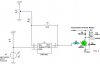
Hi! In the picture that i get from the net, on the right part is for the light sensor and on the left part is the relay driver. I found out that the relay will always trigger eventhough after i change R1 with R2(theoretically it will become a dark sensor). What i understand is, if theres light, dark sensor will not trigger the relay because the resistance will increase. The LDR that i used gives around 1.5kohm when theres light and 10kohm when its dark. Whats wrong with it?
 

Attachments

  • lightsensor.jpg
    lightsensor.jpg
    25.5 KB · Views: 1,064
R1 and R2 create a voltage divider.

You can find out the voltage running into pin 3 of the LM311 comparator by using this equation:

Pin 3 input voltage = (R2 / (R1 + R2)) * voltage (which is 12)

A potentiometer in your arrangement can be a voltage divider as well.

here is another equation that can be used to your advantage:

Pin 2 input voltage = (R1 + R4) / ((R1 + R4) + R3) * vref

vref is the voltage coming out of the middle pin of the potentiometer. so if the potentiometer is set in the middle, the voltage is 6.

A comparator is supposed to compare two voltages.

and are you sure you wired your comparator correctly? I haven't usedthat particular chip number before.

and can someone explain why the 1N4001 is connected between collector and emitter of the NPN? I think it is odd.
 
Hi, this should work if everything is wired good and all components are good.
Of course LM311 needs the +12V on pin8, and needs GND both on pin4 and pin1, but I think you wired all that up, didn't you.

My only comment on the circuit: If the dark resistance of the photocell can be as high as 10kOhm, then I would double R1, e.g. put there 2.2kOhm instead of 1kOhm. Otherwise the input voltage range of the LM311 may be exceeded.

No need to swap R1 and R2 for testing. The tripping point can be adjusted with the R5 pot. Turn R5 toward the minimum (i.e. the resistance between the grounded end of the pot and the wiper of the pot goes to min.), and the LM311 comparator should switch off the relay at a point.

If the circuit won't improve, check the polarity of D2. Or you'd better remove D2. I think there is no reason for it in this circuit.

The normally open (NO) output terminals of the relay should be used for the load.

For the long run:
See to it that the relay is rated for enough current (depends on what the load will take maximum).

Good luck!
 
, on the right part is for the light sensor and on the left part is the relay driver
are you sure about this? :lol:

according to LM311N datasheet max. voltage is 36V. I don't see why increasing voltage from 12 to 15V would make this work any better.
All this chip does is compare two inputs and change output if one is bigger than the other.
 
It also works from +/-12V or, or +/-15V, but these changes do not make any difference as for the functioning of the circuit.
If it won't work from +12V alone, it won't work from +/-12V or from +/-15V either.

The LM311 does not require a split power supply in this application.
So it is less complicated and there are less chances for failure with only a single supply (+12V, GND), so there is no need for -12V or -15V at all.

Tell us what's the odds.
 
Has anyone noticed that LM311 is open collector, and so needs a pull-up resistor on the output? See below.
 

Attachments

  • lightsensor.png
    lightsensor.png
    82.7 KB · Views: 912
mstechca said:
R1 and R2 create a voltage divider.

You can find out the voltage running into pin 3 of the LM311 comparator by using this equation:

Pin 3 input voltage = (R2 / (R1 + R2)) * voltage (which is 12)

A potentiometer in your arrangement can be a voltage divider as well.

here is another equation that can be used to your advantage:

Pin 2 input voltage = (R1 + R4) / ((R1 + R4) + R3) * vref
Why is R1 in your equation for pin 2? That equation makes no sense.

vref is the voltage coming out of the middle pin of the potentiometer. so if the potentiometer is set in the middle, the voltage is 6.

A comparator is supposed to compare two voltages.

and are you sure you wired your comparator correctly? I haven't usedthat particular chip number before.

and can someone explain why the 1N4001 is connected between collector and emitter of the NPN? I think it is odd.
You're correct, mstecha. It serves no purpose.
 
Has anyone noticed that LM311 is open collector, and so needs a pull-up resistor on the output?
You've hit the nail on the head, Ron!
Shame on me how I missed on that one!
Hey, Rubberlele, load Ron's 2.2k into the machine for the good!!!

Yet pretty strange! Rubberlele wrote the relay was always on. The missing pullup alone would set the relay permanently OFF, wouldn't it?

Still remains some incorrect wriring, or something?
 
gerenis said:
Has anyone noticed that LM311 is open collector, and so needs a pull-up resistor on the output?
You've hit the nail on the head, Ron!
Shame on me how I missed on that one!
Hey, Rubberlele, load Ron's 2.2k into the machine for the good!!!

Yet pretty strange! Rubberlele wrote the relay was always on. The missing pullup alone would set the relay permanently OFF, wouldn't it?

Still remains some incorrect wriring, or something?
Maybe he's using the NC contacts on the relay.
 
here is another equation that can be used to your advantage:

Pin 2 input voltage = (R1 + R4) / ((R1 + R4) + R3) * vref

Ron asks:
Why is R1 in your equation for pin 2? That equation makes no sense.

This "R1" is the R1 that represents the 5.6K resistor (coupling resistor).
The diagram must have confused you, and you added to the confusion, because there are now 3 R1's! :lol:

pin 1 will be to ground, pin 4 is -12V and pin 8 is +12V. Im thinking of using +-15V. Is it possible?
Yes, if the voltage does NOT exceed the maximum voltage of any one component. I can't see that increasing the voltage will benefit the circuit.

..., and so needs a pull-up resistor on the output?
I suggest that this (or using a pull-down resistor) should be done to all IC inputs that are not connected to either an IC output, ground, or VCC.
This helps prevent erratic behaviour.
 
This "R1" is the R1 that represents the 5.6K resistor (coupling resistor).
The diagram must have confused you, and you added to the confusion, because there are now 3 R1's!
Still that equation cannot be correct.
To start with: the positive feedback through R4 sets a hysteresis to prevent oscillation during the transition phase of the comparator. Hysteresis means there will be 2 different voltages on pin2 depending on the state of the comparator output (low or high). If you want to give correct description for the pin2 voltage, you should give 2 equations at once, and then also give the third equation which describes in which condition does the first or second equation apply. So that's becoming a bit more complicated...
Practically, I don't see much use for calculating the pin2 voltage, since it can be adjusted to anywhere between GND and VCC with the R5 pot.

I suggest that this (or using a pull-down resistor) should be done to all IC inputs that are not connected to either an IC output, ground, or VCC.
This one doesn't much belong to the topic. I see no floating input problem in the posted circuit. (Mstecha: Yes, unused logic IC inputs should be hardwired to a logic level, VCC or GND as appropriate. Wouldn't say that for all kind of IC inputs though. Consult the datasheet of any particular IC and see what they recommend for each of the unused inputs.)
 
gerenis said:
This "R1" is the R1 that represents the 5.6K resistor (coupling resistor).
The diagram must have confused you, and you added to the confusion, because there are now 3 R1's!
Still that equation cannot be correct.
To start with: the positive feedback through R4 sets a hysteresis to prevent oscillation during the transition phase of the comparator. Hysteresis means there will be 2 different voltages on pin2 depending on the state of the comparator output (low or high). If you want to give correct description for the pin2 voltage, you should give 2 equations at once, and then also give the third equation which describes in which condition does the first or second equation apply. So that's becoming a bit more complicated...
I was ignoring the IC when I was doing the equation. It is obvious that anything positive applied to the base of the NPN will turn on the emitter, so I made that a short circuit during the equation. Basically, for a voltage divider equation, I added R1 and R4 (feedback), and treated it as a single grounded resistor. the resistor connected between the potentiometer and R4 is treated as a resistor connected to the voltage that was calculated or measured at the center of the potentiometer. so then the equation crunches down to (resistor / (resistor + R4)) * center, where center is the voltage coming from the potentiometer center.

Practically, I don't see much use for calculating the pin2 voltage, since it can be adjusted to anywhere between GND and VCC with the R5 pot.
Calculating two input voltage is important in order for the comparator to work for you. a comparator compares input voltages, doesnt it? :wink:
 
mstechca said:
I was ignoring the IC when I was doing the equation. It is obvious that anything positive applied to the base of the NPN will turn on the emitter, so I made that a short circuit during the equation. Basically, for a voltage divider equation, I added R1 and R4 (feedback), and treated it as a single grounded resistor.

That's why everything you said was complete nonsense! - you can't 'ignore the IC', that's what makes the circuit work. Adding R1 (the second R1) and R4 makes no sense either, because they are NOT in series - unless the IC isn't there, when nothing works anyway.
 
Calculating two input voltage is important in order for the comparator to work for you. a comparator compares input voltages, doesnt it?
Yes, the calculation is very easy. The result is:
pin2 voltage can be anything from approx. 0V to nearly +12V, depending on the setting of R5.

In fact the actual range on pin2 extends from a few tens of mV's above 0V to a few hundreds of mV's below +12V, as the comparator output cannot swing all the way to the supply rails. This limited swing has some minor effect back to the pin2 through the 10k-100k resistor divider.

(E.g. the high output voltage of the comparator will be limited to about (12V-0.7V)*5.6k/(2.2k+5.6k)+0.7V = approx. 9V. This would allow the pin2 voltage up to (9V-12V)*10k/100k+12V = 11.7V, not any higher.
But who cares for this hairsplitting?)

As a side-effect I have also calculated the approximate hysteresis voltage on pin2: (9V-0V)*10k/100k = 0.9V.
 
Status
Not open for further replies.

Latest threads

Back
Top