I have designed a 4-layer board which is 96% analog and is about 242mmx70mm in size. It has ±5VDC power supply. The current consumption on each rail shouldn't be more than 500mA, no ground pour on top layer
Having a bit of a hard time deciding on which stackup I should go with. There are 8 identical sections of schematic here which each section input being ~50MHz analog that is connected to a buffer and goes through a 10MHz LPF. Here are what I came up with
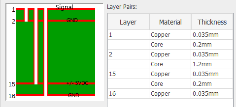
Option1: Split power plane on Ly3 as below with 0.5mm gap between split planes and a few traces crossing the splits

Stackup-

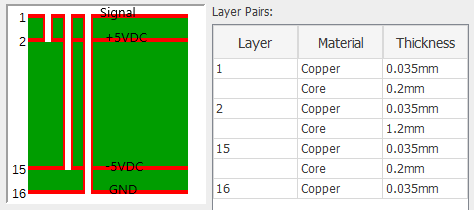
Option2:- Solid power planes stackup as below

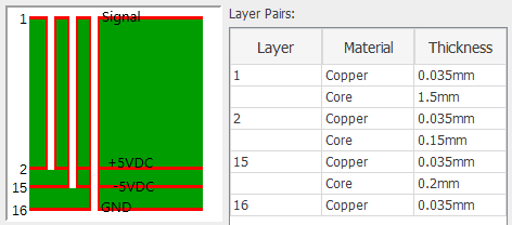
Option3: SOlid power planes stackup as below

Would appreciate any recommendations/suggestions
thanks
Having a bit of a hard time deciding on which stackup I should go with. There are 8 identical sections of schematic here which each section input being ~50MHz analog that is connected to a buffer and goes through a 10MHz LPF. Here are what I came up with
Option1: Split power plane on Ly3 as below with 0.5mm gap between split planes and a few traces crossing the splits
Stackup-
Option2:- Solid power planes stackup as below
Option3: SOlid power planes stackup as below
Would appreciate any recommendations/suggestions
thanks
Last edited:
