Continue to Site

Welcome to our site!

Electro Tech is an online community (with over 170,000 members) who enjoy talking about and building electronic circuits, projects and gadgets. To participate you need to register. Registration is free. Click here to register now.

  • Welcome to our site! Electro Tech is an online community (with over 170,000 members) who enjoy talking about and building electronic circuits, projects and gadgets. To participate you need to register. Registration is free. Click here to register now.

power supply

Status
Not open for further replies.
Oblong,
Just looking at your circuit, there are some inconsistances.

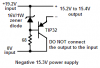
What does U9 and R14 do?

Why are you using a 1% tollerence valuefor R14?

U20 is backwards.

What does C6 do?

What's the point of R7 and why is it 3R5 which is not a standard resistor value (unless you can get E384 values which I've never seen)?

What does R13 do?

2pF is nothing on top of the huge gate capacitance of the MOSFET?
 
Hero999 are you unfamiliar with a standard P-MOSFET LDO topology? Let me provide a less cluttered schematic.

**broken link removed**

You did not read my response “The schematic is a bit messy because I’m bouncing between AC simulations for loop gain and transient for load step testing”. This should explain the function of U9 R14 and R13. C2 is the output cap R7 is the esr. The only components set in stone at this point are the feedback network R1 and R2 standard CRCW 0603 1% thick film resistors. As to C9 read my edit, again this to is not the final value.

Your probe probably has more capacitance then the Cgs of the NTR0202PLT1.:) The effective capacitance off the top of my head it's only about 60pf.

Thanks for your feedback.
 
Last edited:
All you need is an EA that can operate off your rail voltage,pass transistor, a reference and some passives.

Here is a 5.1V nominal LDO I’m building 15 mA max output. The schematic is a bit messy because I’m bouncing between AC simulations for loop gain and transient for load step testing. I’m using a P-FET to minimize ground (Quiescent) current and drop out voltage. V3 is really a TLVH431 reference. You could use the second opamp in the package for current sensing use this with a comparator to shut down the regulator in the event of a sustained OC. You of course have to make sure all components are properly rated for your voltages etc. Anyway the schematic is one possible way of using your desired PNP.

If you have the headroom you are better off using a NPN or depending on available voltages an N-FET. Or as suggested the best solution's a three terminal off the shelf regulator.The data sheets will show how to use a pass Transistor and may have hints for Fold back or basic current limiting.

It’s odd with an EE degree you don’t know how to use an external PASS transistor with off the shelf three terminal regulators 723 ,7800 series etc. Most of these three terminal packages will be thermally limited.
Edit C6 isn't connected to the EA output it should be connected to the bottom of R1.

**broken link removed**


The OP never said he had a EE. He's a graduate of a community college. An AAS is what he probably has. If you've never gone to a community college, it may be hard for you to understand about the low quality instruction you sometimes get. It may be worse where he's at.:)

I think your circuit is a tad bit more complex than what the OP is looking for.
The simplified one you posted would make more sense to him, although it's still not a PNP (I made the same mistake.:)).
 
Last edited:
hey I've a BEng in electronics and communications ,im graduated from a university but its private , i thought community college in usa is as same as our private university in egypt :) , the problem is we have a low quality education , and the instructor not well knowledgable , guess that all the PHDs in electronics who taught us the courses never touched the art of electronics book ? they just know jacob milman and sedra's book , and 90% of them never understood sedra's book , that's why im not very well at EE but im trying to learn from you :). also i didnt get my answer , how do i connect i make a current sink using a PNP instead of an NPN emitter follower .
Really i didnt understand oblong's circuit :D .. its so hard for me :).
 
I do not know what is a "sinking" power supply.
Here is the same power supply that uses a PNP transistor. It is a negative power supply.
 

Attachments

  • negative power supply.PNG
    negative power supply.PNG
    6.8 KB · Views: 161
Hi, audioguru ,
What i mean is or you may correct my confusion ,the NPN approach is sourcing current to the load ? But while using the PNP is like a sink ? or that is only for a switch transistor ? also is that transistor working in active mode ?? it ampilifies the zener's current ?
i know these are basic questions ... sorry ^_^
 
The NPN sources positive current to the load.
The PNP sources negative current to the load.

The transistor is a linear emitter-follower. Its emitter voltage is about 0.7V (the base-emitter voltage) from the voltage of the zener diode.
 
yes , but what i know that the transistor is either in active mode ( amplifier ) or saturated one or cutoff , is this in an active mode ?

What i understood is that you use an emitter follower to let the base (zener's voltage) be like the emitter ( the output) minus the VBE drop but at hight current ( IC ) ?

Yes, the transistor, since it has drop-out voltage is in active mode.
The zener diode controls the regulation of the transistor.
 
hey I've a BEng in electronics and communications ,im graduated from a university but its private , i thought community college in usa is as same as our private university in egypt :) , the problem is we have a low quality education , and the instructor not well knowledgable , guess that all the PHDs in electronics who taught us the courses never touched the art of electronics book ? they just know jacob milman and sedra's book , and 90% of them never understood sedra's book , that's why im not very well at EE but im trying to learn from you :). also i didnt get my answer , how do i connect i make a current sink using a PNP instead of an NPN emitter follower .
Really i didnt understand oblong's circuit :D .. its so hard for me :).

Sorry ahmedragia21, no offense. When you said it was a community college (2 year college), I just assumed.:eek: I didn't see any mention of EE.
 
Hero999 are you unfamiliar with a standard P-MOSFET LDO topology? Let me provide a less cluttered schematic.

**broken link removed**
Yes I am familiar with the standard P-channel LDP topology. I was wrong about the MOSFET being backwards but the schematic isn't drawn to the standard convention of having the power supply on the left hand side which probably confused me.

You did not read my response “The schematic is a bit messy because I’m bouncing between AC simulations for loop gain and transient for load step testing”. This should explain the function of U9 R14 and R13. C2 is the output cap R7 is the esr. The only components set in stone at this point are the feedback network R1 and R2 standard CRCW 0603 1% thick film resistors. As to C9 read my edit, again this to is not the final value.

Your probe probably has more capacitance then the Cgs of the NTR0202PLT1.:) The effective capacitance off the top of my head it's only about 60pf.

Thanks for your feedback.

It suddenly makes sense now.

I still don't see how C8 makes any difference because 2pF is only 3.333% of 60pF and the gate capacitance probably has a much wider tolerance than this.
 
Last edited:
Status
Not open for further replies.

Latest threads

New Articles From Microcontroller Tips

Back
Top