Continue to Site

Welcome to our site!

Electro Tech is an online community (with over 170,000 members) who enjoy talking about and building electronic circuits, projects and gadgets. To participate you need to register. Registration is free. Click here to register now.

  • Welcome to our site! Electro Tech is an online community (with over 170,000 members) who enjoy talking about and building electronic circuits, projects and gadgets. To participate you need to register. Registration is free. Click here to register now.

PNP or NPN Transistors

Status
Not open for further replies.

weegee

New Member
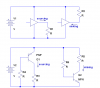
It would seen that most circuits use NPN transistors rather than PNP. I understand the difference between the function of the two, and also the manufactering of the two.

But why are PNP transistors the ugly step sister?!?!?

can someone tell me what the main benefits and uses are for each type (pnp/npn - before someone tries to list every transistor ever made :p)
 
You're probably missing the point?, it's down to manufacturing processes.

Originally PNP transistors were the most common, back in the germanium days, as they were easier and cheaper to manufacture - when silicon took over it switched, because it was easier and cheaper to make NPN ones in silicon.
 
so are there any specific reasons apart from cost where you would use one rather than the other. is there anything that a npn can do that cant be achieved with a pnp or vice versa?
 
It also has to do with majority carrier mobility. The majority carrier in NPN is the electron, while in PNP it is the hole. Electron mobility is considerably higher than that of holes, meaning that NPNs can have higher speed than PNPs.
 
weegee said:
so are there any specific reasons apart from cost where you would use one rather than the other. is there anything that a npn can do that cant be achieved with a pnp or vice versa?
Two examples where PNP or P-channel are often used: Push-pull outputs and motor drives (e.g., mosfets) on the top side. John
 
This is why N-channel MOSFETs generally have a lower on resistance than N-channel MOSFETs
 
Hero999 said:
This is why N-channel MOSFETs generally have a lower on resistance than N-channel MOSFETs

you probably mean that P-channel have lower on resistance than N-channel right? :p :)
 
whiz115 said:
you probably mean that P-channel have lower on resistance than N-channel right? :p :)

No, N-channels have lower resistance than P-channels.
 
Also, they can make N type silicon thinner than P silicon and still have the same characteristics.
 
How about this:

You can use a NPN to sink a device.

You can ony use a PNP to source a device if the base voltage is >= the collector voltage. If it is not you need to use a totem pole setup (2 transistors) which is more expensive.
 
3v0 said:
How about this:

You can use a NPN to sink a device.

You can ony use a PNP to source a device if the base voltage is >= the collector voltage. If it is not you need to use a totem pole setup (2 transistors) which is more expensive.

Doesn't make much sense? - you can use a PNP device to sink current, or an NPN to source it - it's merely a question of the polarity of your supplies.

Don't make the mistake of assuming all supplies are negative earth.
 
Nigel Goodwin said:
Doesn't make much sense? - you can use a PNP device to sink current, or an NPN to source it - it's merely a question of the polarity of your supplies.

Don't make the mistake of assuming all supplies are negative earth.
I don't see what supply polarity has to do with anything. A PNP can only sink significant current as an emitter follower.
 
Nigel Goodwin said:
Reverse the supply and use PNP instead of NPN and it will sink or source just the same - there's no relationship between polarity and sink or source.
Can you show us a schematic of how a common emitter PNP can sink current? I don't understand what you are saying.
 
It hardly needs a schematic?.

Emitter to chassis (+ve), base to switching signal (via a resistor), collector via load to -ve supply. Apply -ve voltage to base, transistor switches ON, and current sinks through the transistor to chassis.

Exactly as you would an NPN, just with the supply reversed.
 
Nigel Goodwin said:
It hardly needs a schematic?.

Emitter to chassis (+ve), base to switching signal (via a resistor), collector via load to -ve supply. Apply -ve voltage to base, transistor switches ON, and current sinks through the transistor to chassis.

Exactly as you would an NPN, just with the supply reversed.
I think you are using different definitions for sourcing and sinking than I am.
EDIT: It's about direction, and not about how ground is defined.
 

Attachments

  • sourcing sinking.PNG
    sourcing sinking.PNG
    18.2 KB · Views: 346
Nigel Goodwin said:
No, exactly the same - flip your diagrams upside down - then the PNP sinks, and the NPN sources.
You can't get significant (conventional) current to flow into (sinking) the collector of a PNP, or vice-versa for an NPN.
 
Roff said:
You can't get significant (conventional) current to flow into (sinking) the collector of a PNP, or vice-versa for an NPN.

Why are you concerned about conventional current flow?, electron current flow is just as valid - like I said earlier, don't get stuck in the 'HT rails must be positive of chassis' syndrome. A negative HT rail and sinking electron current flow is no different.
 
Nigel Goodwin said:
Why are you concerned about conventional current flow?, electron current flow is just as valid - like I said earlier, don't get stuck in the 'HT rails must be positive of chassis' syndrome. A negative HT rail and sinking electron current flow is no different.
I'm not concerned about conventional flow. I just wanted to be sure we were on the same page. And I still want to see a schematic of how you expect to get a PNP common emitter stage to sink current.
 
Status
Not open for further replies.

Latest threads

Back
Top