Hi all,
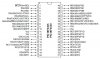
I am doing an analog to digital program. The analog input is set to AN0 and the digital output is port D. The program worked, but bit 7 is starting from bit 3 i.e. shifted by 4 bits (see attached pic). Does someone know what is causing this? The coding is set to left justified since i only need to use the first 8bits.
Below is the coding:
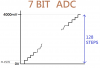
And can someone explain to me what exactly T[SUB]AD[/SUB] means and how to determine which one to use?? and how to determine the conversion clock select bit? (see attached pic)
Thanks in advance,
Adrian
I am doing an analog to digital program. The analog input is set to AN0 and the digital output is port D. The program worked, but bit 7 is starting from bit 3 i.e. shifted by 4 bits (see attached pic). Does someone know what is causing this? The coding is set to left justified since i only need to use the first 8bits.
Below is the coding:
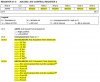
Code:
;REGISTER DECLERATIONS

REG1 EQU 60H ; HERE WE ARE NAMING THE GENERAL PURPOUSE REGISTER


ORG 0000H

;ALL INTIALIZATION HERE OF ALL PORTS AND PERIPHERALS HERE

MOVLW B'00000001' ; SET AN0 AS ANALOG INPUT AND SWITCH ON ADC MODULE
MOVWF ADCON0

MOVLW B'00111110' ;SET AN2 AND AN3 AS REFERENCE VOLTAGES, AND SET AN0 AS ANALOG INPUT
MOVWF ADCON1

MOVLW B'00101100' ;SET AS LEFT JUSTIFIED, SET AS 12 TAD, SET AS FOSC/4
MOVWF ADCON2

CLRF PORTD ;DECLARE PORT D AS OUTPUT FOR THE DIGITAL OUTPUT
CLRF TRISD


MOVLW B'111111' ;DECLARE PORT A AS INPUT FOR THE ANALOG INPYT
MOVWF TRISA

;START MAIN PROGRAM HERE


MAIN


CALL ACQ_DELAY ;CALL DELAY
BSF ADCON0,1 ; CONVERSION IN PROCESS (START CONVERTING)
LINE1
BTFSC ADCON0,1 ;check if ADCON0 bit 1 if clear,if yes skip the next instruction
BRA LINE1
SWAPF ADRESH,W ;MOVE VALUE FROM AN0 TO WORKING REGISTER
MOVWF PORTD  ;MOVE VALUE IN WORKING REGISTER TO PORTD
GOTO MAIN

ACQ_DELAY
MOVLW .3
MOVWF REG1
ACQ1
DECFSZ REG1
BRA ACQ1
RETURN


END_OF_PROGRAME
And can someone explain to me what exactly T[SUB]AD[/SUB] means and how to determine which one to use?? and how to determine the conversion clock select bit? (see attached pic)
Thanks in advance,
Adrian
")