Hi all!
I think I know what's going on in my circuit but I'd like a second opinion (or third, or fourth..") ).
).
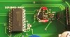
I'm using a p-channel enhancement mode mosfet, ST Micro STS3DPF60L, which is a dual mosfet in an SO-8 package. Datasheet is here, there is a quick schematic of it on the front page: **broken link removed**
Now, I placed this guy on the high side of a load (LED array) to switch the power to the LEDs on and off.
With +4.92v to the gate, I get 4.92v on the source, which is what I want.
However, when I apply 0v to the gate, I get 4.38 or so volts on the source, and the LEDs are still on, albeit a tiny bit dimmer.
This is about 0.54-0.55 volts loss, even though it's supposed to be closed off and 0v. So I look at the datasheet and the protection diode is pointing from drain to source. Since this voltage loss is very similar to what a diode would give, is this the protection diode that's screwing up my circuit and powering stuff even when the gate is off?
If so, can you even switch a load high-side with this kind of part, or no? I need something without a protection diode I'm assuming?
Thanks,
Ray
I think I know what's going on in my circuit but I'd like a second opinion (or third, or fourth..
).I'm using a p-channel enhancement mode mosfet, ST Micro STS3DPF60L, which is a dual mosfet in an SO-8 package. Datasheet is here, there is a quick schematic of it on the front page: **broken link removed**
Now, I placed this guy on the high side of a load (LED array) to switch the power to the LEDs on and off.
With +4.92v to the gate, I get 4.92v on the source, which is what I want.
However, when I apply 0v to the gate, I get 4.38 or so volts on the source, and the LEDs are still on, albeit a tiny bit dimmer.
This is about 0.54-0.55 volts loss, even though it's supposed to be closed off and 0v. So I look at the datasheet and the protection diode is pointing from drain to source. Since this voltage loss is very similar to what a diode would give, is this the protection diode that's screwing up my circuit and powering stuff even when the gate is off?
If so, can you even switch a load high-side with this kind of part, or no? I need something without a protection diode I'm assuming?
Thanks,
Ray