Continue to Site

Welcome to our site!

Electro Tech is an online community (with over 170,000 members) who enjoy talking about and building electronic circuits, projects and gadgets. To participate you need to register. Registration is free. Click here to register now.

  • Welcome to our site! Electro Tech is an online community (with over 170,000 members) who enjoy talking about and building electronic circuits, projects and gadgets. To participate you need to register. Registration is free. Click here to register now.

OR Gate & Relay Circuit

Status
Not open for further replies.

critter4511

New Member
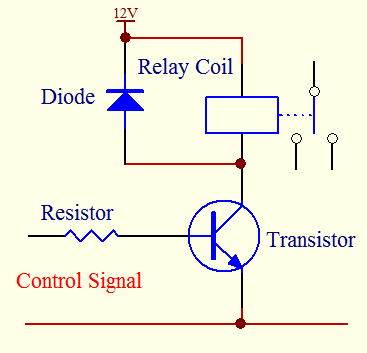
I've built an OR gate circuit to trip a relay. What I want is when any one of the 3 inputs have 5vdc, or a logic high, the OR gate will output 5vdc to the transistor which will trip the relay. It all seems to work until I start adding the actual wiring to the input pins of the OR Gate/circuit board. Just attaching a wire, either by soldering or just touching it to pins 1, 2 or 13, with NO voltage present will trip the relay. Pin 11 will show about 2.5v - 2.8v, and the relay chatters quickly. Desolder the wire or remove it and it all stops. When the wires are attached, there seems to be just enough voltage to turn the 2N2222 on and off quickly. Applying 5vdc directly from the power source to any of those pins with a jumper makes the circuit function properly. So why does just touching or attaching a wire to pins 1, 2 or 13 cause any voltage to be present at pin 11?
1108 Relay.gif
 
Hy critter,

Welcome to ETO.

Your problems are classic. :) The SN74AC32N is a CMOS chip with an extremely high input impedance. As a consequence open circuit wires will easily pick up any electromagnetic signals in the area. This can be radio stations or static electricity. In addition an open circuit wire can cause oscillation where the output of a gate feeds back to the input. This is especially a hazard with non inverting gates like the 74AC32. As you say that you are measuring 2.5V in places, that is exactly what an oscillating chip would indicate.

There are two practical solutions:

(1) Decouple and isolate the chip- a lot of messing about.
(2) Remove the 74AC32 from the circuit and put it back in your spares box and turn the 2N2222 transistor into a three input OR gate, which will be orders slower and less sensitive.

I will post a schematic to turn the 2N2222 into a three input OR gate in a few minutes.

spec
 
Last edited:
Thanks Spec! Your explanation describes exactly what I'm seeing. Can't wait for your design using the 2N2222's. It should be much more stable.
 
This is also called "floating" :) I sometimes place high value resistor for either pull-up or pull-down so input is never floating (I fried one chip that went oscillating due floating situation.....)
 
Fezder...........So you would place a high value resistor at the input pins of 1, 2 & 13? What value would you suggest?
 
Hy again critter,

Here is the circuit that I would recommend.

You can add as many inputs as you like.

C1 probably won't be needed but it helps filter any pickup.

The 100nF minimum capacitor (ceramic) is for decoupling: to short hash picked up on the supply line to 0V and also to lower the impedance of the supply line at high frequencies.

spec

ISSUE o2 2016_04_20


2016_04_18_Iss01_ETO_NOR_GATE_RELAY_DRIVER_VER_1_Sh1.png

ERRATA
(1) Connect a 1N400x rectifier diode cathode to 5V line and anode to collector of Q1
(2) Connect a 1N400x rectifier diode anode to 0V line and cathode to collector of Q1
 
Last edited:
Critter, If you wan't to try that method, pullups/downs are mostly several kiloohms, 4.7k-20k, but I do sometimes use as low as 1k, but for this situation 10k or so should be adequate. Since circuit acts on HIGH, place resistors as pull-down like in this manner:
 
Spec, that circuit looks neat, much simpler than I'd thought :eek:. Does that work in so when there is no voltage input to diodes, they act as open-circuit, and transistor has base-pull-down resistor?
 
And critter, another tip; place catch-diode for relay back-emf, little insurance for transistor :)
(diode is not wrongly placed, it must be reversed so to say)
diode_as_back_emf_protection.png
 
Fezder.......I originally had a diode in place just like you suggested, but it made the transistor and relay go crazy. Don't know if it was related to the operation of the OR gate or not.
 
hmm? diode shoudn't cause any drama, what diode was it? if it was zener by mistake that could do funny stuff
 
VERY odd, does it work without that gate-ic? (7432)
 
Spec, that circuit looks neat, much simpler than I'd thought :eek:. Does that work in so when there is no voltage input to diodes, they act as open-circuit, and transistor has base-pull-down resistor?
Hy fezder,

You can either take the inputs to 0V or leave them open circuit to turn the transistor off.

To turn the transistor on you need to make the input higher than about 2V, so there is a margin for noise.

The 74AC32 OR gate approach for this application is fraught with all sorts of problems, and to make it bullet-proof you would probably need to do a new layout, decouple the supply lines and slug the inputs. But as the OR gate is fast and also non inverting, you only need to get a sniff of the output fed back to the input to get a nice oscillator at typically between 2MHz and 50MHz. It is even worse than that though, because one gate feeds another, which means that the gain is squared.

After looking at that approach, I came to the conclusion it would be easier and safer to remove the gate, which is the main source of the problems.

I don't mean to be critical of the OPs design, because logically it is correct and well thought out, but the inputs of two unused gates are floating and those gates will probably be hooting too. :(

spec

74AC32 Data Sheet
https://www.ti.com/lit/ds/symlink/sn74ac32.pdf
 
Last edited:
I didn't try it........I will however. Thanks.
No probs critter,

I hope my circuit works OK- it should. :)

The trouble with electronics is that schematics do not reflect what is going on in the real word: a piece of wire is an inductor and an antenna, a solder joint is a resistor, and there are small parasitic capacitances associated with all points of any circuit. This even applies to the circuit in the integrated circuit package, where, for example, the fine bonding wires are small resistors and inductors and there are substrate parasitic diodes all over the place. These parasitics would not normally cause a slow speed circuit any problems, but the OR gate you have used is very high speed and, to make matters worse, has an extremely high input impedance. By the way, these characteristics are desirable for logic gates, but they do mean that the layout is critical.

As a general rule, all unused elements in an integrated circuit package: gates, comparators, opamps, etc, must be in a defined state or they may act strangely. Once again, oscillation is possible. With logic, it is normally sufficient to connect inputs to 0V. You may think why bother, the spare elements are not connected to anything so who cares what they do. You would be right, in theory, but, in practice elements often share a common substrate: an oscillating element will take excess current from the supply line, the oscillations may couple to other used elements in the case, and it is possible for an oscillating element to destroy itself and even the complete integrated circuit.

One thing to note, is that logic gates are actually high gain, linear amplifiers over part of their input voltage range. This is also the case for comparators. This is another aspect where schematics do not tell the whole story.

spec
 
Last edited:
If you can get your hands on oscilloscope, that's one big friend on troubleshooting, Critter :)
 
spec, you got any ideas for that diode-phenoma?
 
Status
Not open for further replies.

Latest threads

New Articles From Microcontroller Tips

Back
Top