Continue to Site

Welcome to our site!

Electro Tech is an online community (with over 170,000 members) who enjoy talking about and building electronic circuits, projects and gadgets. To participate you need to register. Registration is free. Click here to register now.

  • Welcome to our site! Electro Tech is an online community (with over 170,000 members) who enjoy talking about and building electronic circuits, projects and gadgets. To participate you need to register. Registration is free. Click here to register now.

opinions on this PCB layout

Status
Not open for further replies.

astronomerroyal

New Member
Hello,

I'm not experienced with PCB layout and I've been spinning my wheels with this one for a while now (see attachements). Was wondering if you could give me your 'first impressions' on the PCB design. I realise this is a lot to ask, so was just hoping for gut-feelings and pointing out egregious errors.

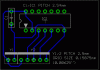
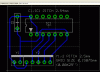
This layout is straight out of the Eagle autorouter, as part of an iterative procedure: autoroute ... make changes ... repeat. Initially, I've been using the number of vias as a 'goodness of layout' metric (down to 37 vias so far, seems acceptable). I've not made any superficial changes, such as spacing traces evenly, or making angles 45degrees...

The gadget is an intervalometer for making time-lapse movies with dSLR cameras. I've linked to a movie at the end.

Microcontroller-centric: two uCs 'Master 18F4620' and 'Slave 18F2520'
All digital (no analogue mixed in)
Power management at top left. Max DC current =150mA. Typically 50mA.
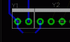
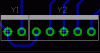
Jacks for camera at left
various headers (ICSP, keypad, various uC pins) along bottom, and top.
When LCD is plugged in to header (at top right), the right side of board is obscured (so no indicator lights, switches can be placed there).
Passes DRC. 100% traces laid. 37 vias.

I've tried to arrange 'functional units' sensibly around the uCs. Been following some tutorials, e.g.
https://www.electro-tech-online.com/custompdfs/2010/02/PCBDesignTutorialRevA.pdf


Q: Is autoroute ... adjust ... autoroute a good way to explore an initial layout? Is number of vias a good quantitative measure of 'goodness of fit'? If so, is there any sort of rule-of-thumb regarding the vias-vs-pins ratio?

Q: Do you know of any pedagogical books that are full of example layouts: idea -> schematic ->layout. I've read a lot of 'common sense' and 'best practices', but am looking for more concrete examples (i.e. hand-holding).

Q: How much do you imagine someone would charge to take my schematic and produce a board layout?


[video=vimeo;7663437]http://vimeo.com/7663437[/video]
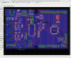
 

Attachments

  • snapshot_PCB_1_feb_14_2010.png
    snapshot_PCB_1_feb_14_2010.png
    212.4 KB · Views: 462
  • snapshot_SCHEMATIC_1_feb_14_2010.png
    snapshot_SCHEMATIC_1_feb_14_2010.png
    74.7 KB · Views: 393
Last edited:
I only had a brief look, but it looks generally quite alright.

I notice there is likely not enough decoupling on the supply (VCC) line. There should be a capacitor close to each VCC of the ICs. It doesn't hurt to use VCC tracks that are a little thicker either. Vias into the ground plane are usually done close the the ground pins of ICs.

There is a servo been supplied poweer from the same vcc; I would suggest placing a bulk capacitor on the supply for the servo. I would also provide some filtering (small resistor (maybe 10 - 22 ohm) to the micro's vcc) between the VCC of the servo and that of microcontroller as there will be some noise present from the servo.

Regarding cost of designing pcbs from schematics, it depends on who's doing it. I would imagine that for something straight forward like the above, $15-$30 would be acceptable for some backyarder, while $75-$150 might be reasonable for some pro. That said, I've never actually used that service so I don't know.
 
Dougy83, thanks for the excellent advice. I get distracted by the details and forget the basics...

EDIT: actually I forgot, the third servo pin isn't VCC but a 'power enable' line that will switch the power on an external servo board. However, I've taken your advice on board, so to speak.
 
Last edited:
How do you intend to make the board? If it's home-etched, you won't be able to do vias, and without a soldermask the between-the-SMD-pads on P2 will probably bridge.

If you're doing 150mA, you might need thicker traces to avoid voltage drops on VCC and GND.

What are the servos for? A simple timer board and LCD would not need all this stuff. What purpose do the servos and light sensors serve?
And putting a Master and Slave chip on a single board may be way too complicated- generally, you'd want to base it on a controller with enough pins and hardware features to do the whole job.
 
Last edited:
Bugger, I was going to use Advanced Circuits' 'Bare Bones' service
**broken link removed**
which doesn't provide a solder mask. I've never soldered an SMD part before. I have some 0.02 solder and very fine tips for my iron; maybe I can just be extremely careful(?).

I shall make power traces as wide as possible - wasn't sure how to get the autorouter to do that autoroutamatically.
 
He's talking about the routes that go between the pins on P1 and P2 and go to R8 thru R11. Just fix them so that they go straight out from the pin rather than up and out between the pins.
 
...putting a Master and Slave chip on a single board may be way too complicated- generally, you'd want to base it on a controller with enough pins and hardware features to do the whole job.

I agree with Oz' on this one. At first glance it seems you should be able to do everything you want to do with just the 18F4620. Drive the LCD in 4-bit mode (save 4 pins) and use the LCD D4..D7 lines as column driver lines for the Keypad (save 4 pins). Are you doin' something really exotic with either one of those processors?

Regards, Mike
 
Make sure you enter in your production service's required clearances as well. Be sure that the Autorouter went to 100%, and check for DRC errors. If Eagle can't route everything, it won't bring up a dialogue box saying so and it's hard to see the unrouted nets. They're not obvious at all unless you change the color.

When you specify a wire Class in the schematic, the Class type has a width associated with it. The autorouter will always use this width. In some cases this is a problem, for example a thick power bus that also feeds the Vdd on a fine-pitch SMD component. Eagle's autorouter can't handle 2 different sizes on the same node and it'll have to be done manually.

Well, you can manually move that thing on P2. It's not even necessary, it could go straight to the pin. The ones going between pads on the inline header are also problems. Sure, you COULD solder it without a problem, but it's difficult and risky. In fact, ALL your stuff here, like the EEPROM, will be difficult to solder without a mask.
 
I agree with Oz' on this one. At first glance it seems you should be able to do everything you want to do with just the 18F4620. Drive the LCD in 4-bit mode (save 4 pins) and use the LCD D4..D7 lines as column driver lines for the Keypad (save 4 pins). Are you doin' something really exotic with either one of those processors?

Regards, Mike
Or a larger package. They're finer pitch, thus more difficult to solder, but well worth it.
 
He's talking about the routes that go between the pins on P1 and P2 and go to R8 thru R11. Just fix them so that they go straight out from the pin rather than up and out between the pins.
Not just that. "Master" has routing that would be next to impossible to avoid bridging without a mask. SOME of it can be fixed.

You have a major bug all through your design due to a mismatch between the Autorouter's Grid size and the pin coordinates. Look on Master. Many of the wires don't come directly off pins, they're offset so the edge of the trace starts to jam BETWEEN pins. This is "messy" for a board with a soldermask, and really bad for a board without a soldermask since it invites bridging.

You can fit this by using a finer Grid size (you will need to Ripup everything rerun Autorouter). Or you can fix it manually by using a fine Grid or Alt Grid size and using the Move tool on each trace to make it align with the pin. Or better yet, you need to manually Ripup each trace as it approaches the pin, then manually Route with the Route mode set to that it aligns with the pad's units and does not Snap to the current Grid until it changes direction.
 
Last edited:
Hi,

first off - did you perform a DRC? I'm worried about many traces in almost direct contact with SMD pads. Eagle uses a standard minimum distance of ~0.20mm for criterium, which I increase to 0.3048mm for my PCB designs.

Secondly you should avoid 90 degree bends in the traces. They don't look good and additionally the traces might be damaged if the PCB gets hot.

A double 45 degree bend can stand a lot more thermo-mechanical stress.

There is no rule of thumb for the number of vias.

My opinion: The higher the number of vias the poorer the design. You can reduce the number of vias by looking at the ratsnest.

Many crossing air wires require complicated routing with probable vias. Considering that fact you might place components for the least amount of crossing air wires before routing.

Very often a trace on the component side turns out to be unnecessary by just repositioning one single component.

When the final design is finished make ground fills on both solder and component side. Ground fills ensure quick and even etching process and last not least mean less poisonous stuff to get rid off for a cleaner environment.

Boncuk
 
Last edited:
He's talking about the routes that go between the pins on P1 and P2 and go to R8 thru R11. Just fix them so that they go straight out from the pin rather than up and out between the pins.

I see, thanks. Shame on the autorouter. Looks like my barely touched illuminated loupe is finally going to see some action.

Are you doin' something really exotic with either one of those processors?

Exotic? Not sure. I'll spare you the long story but the intervalometer does more than simply fire a camera, it also executes 1ms-precision exposures ... for up to four cameras simultaneously. I decided to dedicate the slave 18F2520 to this task, receiving I2C packets from the Master 18F4620, which itself performs a real-time clock as well as the whole user-interface. I gathered requests from time-lapse aficionados. A big request is that the user-interface can be used while the gadget is controlling the camera (i.e. the millisecond timing isn't messed up by the user's fiddling). I tried doing it with TMR0, TMR1 interrupts etc. on one 18F4620 but the simultaneity of it all became a headache, one that was instantly relieved once I did the 2-microcontroller set-up. It was a landmark in my microcontrollin'.

Or a larger package. They're finer pitch, thus more difficult to solder, but well worth it.

I do have some TQFP adapter boards waiting for some 100-pin chips. I just don't know how people actually gain experience with high pin-count projects; they seem so difficult to prototype and the PCBs so expensive to have made. Even the barebones PCBs are going to cost a pretty penny, the only consolation being that the money's going into the US economy, instead of China's.
 
Not just that. "Master" has routing that would be next to impossible to avoid bridging without a mask. SOME of it can be fixed.

You can fit this by using a finer Grid size (you will need to Ripup everything rerun Autorouter). Or you can fix it manually by using a fine Grid or Alt Grid size and using the Move tool on each trace to make it align with the pin. Or better yet, you need to manually Ripup each trace as it approaches the pin, then manually Route with the Route mode set to that it aligns with the pad's units and does not Snap to the current Grid until it changes direction.

That's a pretty time consuming method. It will most likeley bring about new error messages when performing a DRC (angle off). Many components are manufactured on imperial scale. Relays and switches are mostly oriented to metric scale. To combine both on a PCB design use any standard inch-based grid size. When (manually) routing between an off-grid pad and an on-grid pad start the trace at the off-grid pad. The trace will start in the center of that pad. Continue routing until the air wire towards the on-grid pad becomes absolutely straight and finish that trace.

Routing between two off-grid pads start traces from both pads and draw them towards each other. The trace will eventually be on grid, if not on the straight portion, then anywhere after a 45degree bend. Join the trace parts at bends and you'll have the same "presentation" as you have with on-grid elements.

It really works well. Take a look. For the DRC disable "Off Grid". (There are Off-Grid components on the PCB!)

Regards

Boncuk
 

Attachments

  • TRACE-01.gif
    TRACE-01.gif
    12.1 KB · Views: 215
  • TRACE-02.gif
    TRACE-02.gif
    16.1 KB · Views: 214
  • TRACE-03.gif
    TRACE-03.gif
    11.8 KB · Views: 204
  • TRACE-04.gif
    TRACE-04.gif
    20.4 KB · Views: 208
Last edited:
You have a major bug all through your design due to a mismatch between the Autorouter's Grid size and the pin coordinates.
You can fit this by ...

I'll do whatever it takes. I think I changed the grid resolution in order to place parts more precisely, without realizing that it was also going to affect the autorouter. I've literally spent hours autorouting and ripping up this thing, a few more and a final manicure isn't going to be a problem.

Hi,

first off - did you perform a DRC? ... a cleaner environment.

Boncuk

Boncuk, thanks. DRC was passed, rather surprisingly. I'll double check the DRC clearances ... everything is 8mil. My traces are 10mil. Zooming in, it looks as though the clearance on some of the messy traces is at the 8mil limit. I will pay particular attention to this.
I shall add 45degree angles manually, as I near the end. Yes, I've slowly come to realize that untangling the ratsnest has largely been the goal. I've even reassigned microcontroller pins in order to untangle pairs of 'rat twigs'. Ah, it never occurred to me to do the ground fill/polygon after the traces are set down. Does the order affect the autorouter? And yes, I care about the environment.
 
Very nice for first effort. I do the same: autoroute, move components, ripup, and again. I try to use 0.025" grid, and 0.012" traces/spaces. Other widths when necessary.

I also tend to avoid vias beneath any device. On a non-pth board, you need room to solder the jumper. If any part has a metal back it's a disaster.
 
Status
Not open for further replies.

Latest threads

New Articles From Microcontroller Tips

Back
Top