PG1995
Active Member
Hi
Please use this attachment and please help me. Thank you.
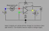
An op-amp tries to make differential voltage across its input terminals zero which also means that no input current flows into the op-amp.
In this case of Figure 12-22, it's easier to understand what is really happening. As Vout = (-Rf/Ri)Vin, therefore when value of Ri is low, the Vout is made more negative so that 'positive charge carriers', i.e. conventional current, are pulled away from the inverting input terminal of the op-amp with greater force and no charge carriers enter into the op-amp.
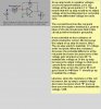
Q: The circuit on the left uses inverting configuration whose gain is given as Vout/Vin = -Rf/Ri.
In the given case Vin is negative therefore Vout = (Rf/Ri)|Vin|.
I'm assuming that the relation for Vout given above is correct. When the resistance of photoconductive cell decreases (which in this case is Ri), the Vout increases. Conceptually, I don't get why an op-amp would increase its Vout as Ri decreases.
Likewise, when Ri increases, Vout will be decreased. Why?
Regards
PG
Please use this attachment and please help me. Thank you.
An op-amp tries to make differential voltage across its input terminals zero which also means that no input current flows into the op-amp.
In this case of Figure 12-22, it's easier to understand what is really happening. As Vout = (-Rf/Ri)Vin, therefore when value of Ri is low, the Vout is made more negative so that 'positive charge carriers', i.e. conventional current, are pulled away from the inverting input terminal of the op-amp with greater force and no charge carriers enter into the op-amp.
Q: The circuit on the left uses inverting configuration whose gain is given as Vout/Vin = -Rf/Ri.
In the given case Vin is negative therefore Vout = (Rf/Ri)|Vin|.
I'm assuming that the relation for Vout given above is correct. When the resistance of photoconductive cell decreases (which in this case is Ri), the Vout increases. Conceptually, I don't get why an op-amp would increase its Vout as Ri decreases.
Likewise, when Ri increases, Vout will be decreased. Why?
Regards
PG