Continue to Site

Welcome to our site!

Electro Tech is an online community (with over 170,000 members) who enjoy talking about and building electronic circuits, projects and gadgets. To participate you need to register. Registration is free. Click here to register now.

  • Welcome to our site! Electro Tech is an online community (with over 170,000 members) who enjoy talking about and building electronic circuits, projects and gadgets. To participate you need to register. Registration is free. Click here to register now.

OP Amp circuit question

Status
Not open for further replies.

jctoday

New Member
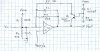
I recently ran into to an OP Amp circuit in which there is a strange negative feefback path that just I counldn't quite figure out what it supposed to do. Would someone please take a look and tell me what could be the purpose of R4, Q1, D1 and R5 circuit doing in the OP amp feedback path? Thanks!
 

Attachments

  • Op Amp schematic.JPG
    Op Amp schematic.JPG
    39.5 KB · Views: 345
Just taking a wild stab... Looks like the transistor is supposed to turn on if Vout goes above Vref, which will pass current back to the inverting input and reduce the output; so it's a clamp (keeps Vout below Vref). It might actually clamp the output a little above or below Vref as the diode voltage and transistor Veb won't necessarily match.
 
You are probably right. The same VREF goes to the ADC REF, I think it's meant to protect the ADC input. I am just wondering why doing it this way instead of using clamping diodes at the input of the ADC.
 
Hello there,

It would help to know where this circuit came from and what it is supposed to do.
The transistor will limit the output without distorting it as much like a clamp diode would, or provide a softer clamp.
Without knowing that this entire circuit is used for however, it could even be a very crude triangle to sine converter for example.
 
Yes the circuit is a clamp.

To a first-order, D1 compensates for the base-emitter voltage of Q1.

They use an active clamp instead of a diode because the clamp has a more accurate and sharper clamp point then a simple diode by itself.

Below is an LTspice simulation of the circuit. Note that you need to add an input resistor for proper operation of the circuit. Notice the sharp clamp point is at 5.19V for V2 (Vref) of +5V.

Clamp.jpg
View attachment Clamp.asc

Edit: An observation: R4 is not really needed and can be replaced with a short.
 
Last edited:
This is almost what I used in an audio limiter.
I used a PNP & NPN to limit + and - levels.
 
This is almost what I used in an audio limiter.
I used a PNP & NPN to limit + and - levels.
That would certainly give a sharp limit to the signal. But if you are listening to the result, a softer limit, such as from a standard diode, would probably give a less strident sound when the audio is being limited.
 
Hi again,

Strictly speaking though it's not really a clamp, it's a gain limiter. It doesnt clamp the gain, it just reduces the gain when the output gets above a certain level.
The 100k resistor forward biases the base emitter when needed. Without that the transistor would not turn on. With it shorted, it will turn on too soon.
Still not telling us what this circuit is currently being used for however.
 
Vbe breakbown is not modeled. When the output swings about 2V below ground (assuming 6V breakdown), there will be nearly a direct short between the op amp output and the reference voltage. Attached is the result of a sim with and without Vbe breakdown. I used a "real" op amp. because opamp.sub does not have output current limiting.
The 100pF caps stopped low-level oscillations.
2N3906.sub has the breakdown modeled. Q2 prefix is QP. Q1 prefix is X.
Below is the subckt that I made. If anyone sees a flaw, or can suggest improvements, please speak up.
Code:
*
.subckt 2N3906 1 2 3
Q1 1 2 3 0 2N3906
D1 2 3 IdealZener6V
.model D D
.lib C:\Program Files\LTC\SwCADIII\lib\cmp\standard.dio
.model NPN NPN
.model PNP PNP
.lib C:\Program Files\LTC\SwCADIII\lib\cmp\standard.bjt
.model IdealZener6V D (Ron=10 Roff=1e12 Vfwd=6)
.ends
 

Attachments

  • feedback clamp.PNG
    feedback clamp.PNG
    30.7 KB · Views: 289
  • feedback clamp.asc
    3.5 KB · Views: 257
Strictly speaking though it's not really a clamp, it's a gain limiter. It doesnt clamp the gain, it just reduces the gain when the output gets above a certain level.
The 100k resistor forward biases the base emitter when needed. Without that the transistor would not turn on. With it shorted, it will turn on too soon.
Clamping the output doesn't mean clamping the gain, it means limiting (clamping) the output to a fixed level, which this circuit clearly does. At that point the gain becomes essentially zero to any further input voltage excursion.

The 100k resistor is to provide bias current through the diode. If you didn't have the diode then you wouldn't need the resistor. You would just connect the transistor base directly to Vbias.
The diode is there to compensate for the Vbe of the transistor.
I think that you and Al have gotten a little crossed up because you referred to eliminating R4 in the original circuit, and he thought you meant R4 in your schematic.
It's all moot, though, unless the output is constrained to prevent Vbe breakdown.
 
Clamping the output doesn't mean clamping the gain, it means limiting (clamping) the output to a fixed level, which this circuit clearly does. At that point the gain becomes essentially zero to any further input voltage excursion.

The 100k resistor is to provide bias current through the diode. If you didn't have the diode then you wouldn't need the resistor. You would just connect the transistor base directly to Vbias.

Hi Carl,

About the 100k resistor, i might have misunderstood you on that, but as far as clamping the output, it doesnt really clamp the output, it limits the gain.
If it was a true clamp it would not have the 10k resistor in series with the collector. That 10k resistor works in parallel with the 43k resistor when the transistor turns on and that causes the gain to decrease, but still does not clamp the output.

Consider this: we apply some voltage on the input (perhaps through a resistor for some input impedance) and we get a gain of 10 with the 43k resistor in place, and the transistor is not on at all yet. Lets say that the input was 0.1v, then the output was 1v. Now lets say we increase the input to a level that turns the transistor on hard. Now the 10k is practically in parallel with the 43k so the gain is reduced to 2. If that took an input of 1v then we would have 2v on the output. Now if we increase that input to 2v we would have 4v on the output. If we again increase that 2v to 4v we would have 8v on the output, etc., etc. Note that at no time did the output get clamped to some set value.
However, if we removed the 10k resistor and replaced it with a short, then we would have a true clamp because the gain would go so low it would always keep the output fixed at some set level which although would still rise slightly with input, it would not rise very much at all so it would look like a clamping circuit.

So the difference between this circuit and a clamp circuit is a clamp circuit would keep the output fixed at some set level regardless of the input, while a gain limited amplifier would reduce the gain but still allow the output to rise with the input voltage level holding some fixed gain. So you could call it a 'gain' clamp i guess :)

I still need to hear from the OP though to find out what they used this circuit for, or what its original intended purpose was.

Amps like these however are also used to provide gain steps to calibrate sensors that have nonlinear output characteristics. There are usually more set points however (more than one transistor and 10k resistor) so the gain changes gradually in steps as the sensor output increases. This helps to linearize the output characteristic of the sensor. This is one of the reasons i suggested a cheap triangle to sine converter because that transistor and 10k resistor can help shape a triangle into a sine. Usually those have provisions for dual polarity signals however, so before i'd believe that i think i would believe it is a sensor set point calibrator circuit.
 
Last edited:
Mr Al, the transistor never saturates in Carl's simulation, or in mine, so the 10k collector resistor has no effect.

As I pointed out, and everyone is ignoring, the circuit will not work, except at low voltages, because of Vbe breakdown.
 
Last edited:
Hi crustschow, In your simulation in post #5, the output wave (blue) shows -21v. From where this voltage came ?
My op amp is an ideal device and has no voltage limit. In the real world the voltage would be limited to the supply voltage or less.
 
MrAl, as Roff noted the 10k resistor (R4 in the original schematic, sorry for the confusion with two R4's) has no significant effect on the clamp. It does not provide variable gain. You can remove the resistor and the clamp will operate just the same. Your thought experiment is in error. Run the simulation if you don't believe.

And of course, Roff's comment about the base-emitter breakdown is correct.
 
Hi Carl,

Well, it appears to me that if you have a 40k resistor in the feedback path then you have some gain say gain=10. Then, if you parallel a 10k resistor with that 40k resistor you must end up with less gain than 10 in that amplifier stage, but that doesnt means that it will be some near perfectly dead set level like say 5 volts. A clamp would force the output to some set level if it tried to go above that level, like say 5v, while a regular 'gain' change would kick in at say 5v but would only limit the gain above that.
Make sense?

If i do a simulation and parallel a 10k and 40k in the feedback i'll get 8k in the feedback, which tells me that stage will then have less gain than with the 40k. That still doesnt tell me that the output will somehow go to some 'fixed' level as i continue to increase the input.
Make sense to you?

If i remove the 10k resistor i have no doubt it will be a clamp circuit, but the 10k is drawn in the circuit so i dont remove it. If the user wants a clamp circuit they should remove the 10k resistor.

Yes i know about the reverse BE diode issue, but i assume we are ignoring that for the time being just to try to figure out what the author originally had in mind.
 
Last edited:
Well, it appears to me that if you have a 40k resistor in the feedback path then you have some gain say gain=10. Then, if you parallel a 10k resistor with that 40k resistor you must end up with less gain than 10 in that amplifier stage, but that doesn't means that it will be some near perfectly dead set level like say 5 volts. A clamp would force the output to some set level if it tried to go above that level, like say 5v, while a regular 'gain' change would kick in at say 5v but would only limit the gain above that.
Make sense?

If i do a simulation and parallel a 10k and 40k in the feedback i'll get 8k in the feedback, which tells me that stage will then have less gain than with the 40k. That still doesn't tell me that the output will somehow go to some 'fixed' level as i continue to increase the input.
Make sense to you?
It would make sense if the circuit worked as you think it does. But it doesn't. Do the simulation, don't just talk about it.

As soon as the output tries to rise about the transistor's base voltage it will start to apply voltage to the 10k resistor so as to keep the voltage at the base voltage value (in other words clamping it at that level). This will continue until the transistor saturates. Only when the transistor saturates, when the voltage at the 10k resistor reaches the reference voltage level, will the output then start to rise with a new gain value based upon the parallel value of the two feedback resistors.

Make sense to you?:)
 
MrAl, the transistor is active (unsaturated) until about 500uA flows through the 10k collector resistor. When the transistor is active, the 10k resistor has no effect.
With the output at 5V, 116uA (5V/43k) will be flowing through the 43k resistor . This means that the source resistor has to be providing (500uA +116uA)=616uA before the transistor saturates. This would require that the input voltage would have to be more negative than -6.16V in the posted simulations.
 
Status
Not open for further replies.

Latest threads

Back
Top