PG1995
Active Member
Hi
Could you please help me with this query? You can see the complete chapter here. In the attachment I'm referring to the chapter's page number not that of PDF file's page number. Thank you.
PS: The author kind of elaborates on what he really means by "worst-case logic state situations" in second-to-last paragraph on page #325. Example #6.9 on page #331 is also useful where the author says "and transistor sizing will follow the worst-case path approach".
Attachments
Last edited:
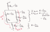
") Let me phrase my question differently. I understand when we have two resistances in parallel then the equivalent resistance is less than both. Let's say low voltage is 0.2V. Why would it be worst case if low voltage increases to 0.4V when only one path path is conducting? In my opinion noise margin can accommodate this little increase in voltage. Do you get me? Thanks for the help.
Let me phrase my question differently. I understand when we have two resistances in parallel then the equivalent resistance is less than both. Let's say low voltage is 0.2V. Why would it be worst case if low voltage increases to 0.4V when only one path path is conducting? In my opinion noise margin can accommodate this little increase in voltage. Do you get me? Thanks for the help.