Electro Tech is an online community (with over 170,000 members) who enjoy talking about and building electronic circuits, projects and gadgets. To participate you need to register. Registration is free. Click here to register now.
Welcome to our site! Electro Tech is an online community (with over 170,000 members) who enjoy talking about and building electronic circuits, projects and gadgets. To participate you need to register. Registration is free. Click here to register now.
Hello all. I have never made my own PCB yet am getting ready to try. When I have to add a VIA between two layers, I know I have to drill a hole, but is there a component/insert of some kind to put in the hole. or can I jill the hole with solder?
You can buy pins that you solder both sides but hobbyists often just use a bit of wire. Most people only do single sided at home, starting with a double sided board is not really a good idea.
ThankX the wire idea is what i was thinking too. The kit I am going to order from digikey.ca comes with both single and double. so i was going to try both. I am just getting prepared now. desighning schematic and PCb in software ext....
Double sided seems like it would be really hard to pull off well..
Getting the positions right would probably be really hard..
Will try it sometime.
Some crucial tips I can give you:
Use glossy photo paper or paper from a magazine.. THIS IS A MUST IMO!!
Crank up the contrast and darkness on your LASER printer.. not inkjet
Use the highest heat setting on your iron .. press very firmly when ironing..
Remember to iron each section equally.. Iron for at least 20 min (depends really)
After ironing soak the board in WARM water for at least 20 minutes..
I find that really cold water makes the paper curl off..
Peel off what paper you can.. rotate your thumb in a circular motion on any paper that sticks.. you can be pretty rough if the toner stuck..
Use warm etchant .. place the etchant in a plastic bowl with the copper clad board..
The biggest mistake I made was not rocking the bowl during etching.. always keep the bowl rocking back and forth! This speeds etching ten fold..
After the copper which is not covered with toner has vanished.. Wash off the black toner with .. I like to use a rough metal scour .. You can get them at the department store (usually used for washing dishes)
Now I like to use a magnifying glass and very sharp box cutter.. find any shortouts and firmly separate the connect.
I also like to use my multimeter and perform a continuity test on the whole board.. Wouldn’t want to search for discont. after 100's of components are in place!
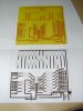
Next, using the original layout on paper and a drill press... I drill out the holes..
Then give it one more clean.. and your ready to populate the board with the components..
I recommend the FREE version of Eagle PCB layout designer by CadSoft
After the board is done.. you can protect the copper from oxidation by spraying silicone comformal coating..
For etching I use Ammonium persulfate with AMAZING results
In the board editor command line. Type POLYGON GND if you want to do a ground fill and your ground is named GND. Or POLYGON VSS if ground is VSS. After that you need to do a RATSNEST and it will finish doing the fill. You can do a polygon for any signal.
The distance from the fill to other signals is controlled by CHANGE>ISOLATE.
Each time you load the board none of fills exist till after you do RATSNEST.
You can route other traces through an existing pour. The next time you do RATSNEST it will adjust the pour.
There are a few goofs I have made more then once. One is to forgot to do RATSNEST prior to printing the board for toner transfer. It will still work if you routed all the polygons signals prior to the pour. If not you circuit will be missing them.
Peter said:
(I wish more people would post there boards, I don't know why but there is something about a PCB to me )
I would guess that most people are not willing to suffer the abuse they imagine their board (or code) will draw or generate. If either is a work in progress say so. They post any changes suggested by others that you use. One of the great things about this site is how well people work together.
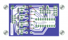
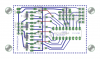
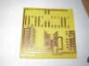
Here is an spread out version (ver 1D) of the Switchboard board after and prior to RATSNEST. Notice that the GND traces have been included in the fill.
EDIT: just saw you post about it working. Good news.
FWIW the 4 targets on the board help me with alignment. I predrill all holes with the CNC prior to etching. To align the toner transfer paper to the board I poke pins through the targets and into the holes on the board. It gets you close and you need to fine tune it from there.
This method would work for the 2nd side of a DS board if you use the etch drill etch method. When doing DS boards I use box/packing tape to protect copper I do not want etched.
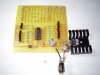
Generally good but I have some contructive criticism to offer:
The resistor leads shoudl be straightened about a bit to make it a bit neater and I'd make them a bit shorter too.
The transistor leads are a bit too short, they should be around 3mm or 1/4" to minimise stress to both the package (during insertion) and the semiconductor junction (during soldering).
Is there some where locally you can get this chemical like home hardware ext. I live in Ontario, Canada. Digikey does not seem to have it in there cataloge.
It is a starter kit, PCB Fab-In-A-Box by a company called Pulsar. Has 20 Sheets TTS, a role of green TRF, White TRF, 2PCS 8"x10" double sided .032", 1/2oz copper boards and 2 same spec. 8"x10" single sided boards.
I didn't buy the laminator they suggest, most of the boards I plane to make are small and I figure I can use a close iron.
I did use a progie called "expressPCB and ExpressSCH" but when you print out the laters they are not mirrored for the board. I will try the eagle program.
This site uses cookies to help personalise content, tailor your experience and to keep you logged in if you register.
By continuing to use this site, you are consenting to our use of cookies.

") )
)