Continue to Site

Welcome to our site!

Electro Tech is an online community (with over 170,000 members) who enjoy talking about and building electronic circuits, projects and gadgets. To participate you need to register. Registration is free. Click here to register now.

  • Welcome to our site! Electro Tech is an online community (with over 170,000 members) who enjoy talking about and building electronic circuits, projects and gadgets. To participate you need to register. Registration is free. Click here to register now.

New PCB: FT232RL USB to serial

Status
Not open for further replies.

edeca

Active Member
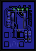
My latest PCB. I haven't had one made yet, will happily incorporate any constructive feedback before I sent it off. It is designed to meet the BatchPCB 2-layer rules.

This implements a number of the features which are described in the FT232R datasheet. I/O voltage is selectable between 5v and 3.3v using the jumper at the top. All serial port pins are exposed to a breadboard through the connector.

LEDs are available to show the status of RX and TX (the chip has a circuit built-in to ensure these are seen even with a brief data transfer).

USB power is provided to the circuit through the 5v connector using a slow start circuit as suggested by the datasheet. This is apparently programmable up to 500mA.

I'm looking forward to testing this chip. The potential of USB (with all versions of Windows and modern Linux kernels) with USB power is quite appealing.

**broken link removed**

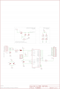
This is my first entirely SMD board. Constructive feedback most welcome.
 

Attachments

  • PCB0009 - Schematic.PNG
    PCB0009 - Schematic.PNG
    68.6 KB · Views: 1,861
It looks like you used the minimum trace width for all your traces. There's no reason to use the minimums here. Up all your trace widths unless it's absolutely necessary. Especially your power traces.

Not certain what that 4.7uf cap is doing. Seems to be in the middle of nowhere. If this is a power cap, it should be inline and not at the end of a branch.

I can see several placements I would change and I would mash it down a little, but they are just finicky suggestions and nothing important. Maybe cut some of the board on the left side. It's okay for the usb connector to hang off the board a little.
 
It looks like you used the minimum trace width for all your traces. There's no reason to use the minimums here. Up all your trace widths unless it's absolutely necessary. Especially your power traces.

Great point. I actually routed them as small as possible just to get the layout. I really should go back and bump some of them up.

Not certain what that 4.7uf cap is doing. Seems to be in the middle of nowhere. If this is a power cap, it should be inline and not at the end of a branch.

I took this from the FT232R datasheet. I would guess it is smoothing the power supply from the USB host, but 4.7uF seems a little small for that. It is there in all of their examples, therefore I kept it.

I can see several placements I would change and I would mash it down a little, but they are just finicky suggestions and nothing important. Maybe cut some of the board on the left side. It's okay for the usb connector to hang off the board a little.

That's also a good point, hanging over might actually be beneficial. Sure, it could be smaller and I have wasted a bit of board space. I'm not too fussy about that though. The entire thing is still only 1" x 2", easy to forget when zoomed in to 20x :)

Thanks for your suggestions.

Someone else pointed out the p-channel FET is actually the wrong way round, so it needs altering anyway. Oops!
 
I took this from the FT232R datasheet. I would guess it is smoothing the power supply from the USB host, but 4.7uF seems a little small for that. It is there in all of their examples, therefore I kept it.

It's not the fact that it's on the schematic, it's the layout that is incorrect. Power caps need to be inline on the power trace with the power running through them or else they lose a lot of their efficiency. You can't branch off a trace and place the cap at the end.

You have to watch out with BatchPCB when components hang off the board. You are charged for the size of your gerber and since the silkscreen for the USB connector is still out to the left, your gerber will still be the same size even though your board edge has moved to the right. In order to get around this, I had to make a custom component and crush the silkscreen down so it didn't extend off the edge.

I'm always finicky about board space. I know it generally means nothing, but I just always like to have everything mashed in, trying not to sacrifice layout. This is an FT232R board I etched myself. It's an absolute minimal board as I only use it for basic Serial/USB at 3.3V. Unfortunately, only problem was that the 4 pin pinhead footprint doesn't have enough annular ring material for a home etched board with not the most accurate hole drilling and I had to do some messy fixing since the pinheader broke those annular ring traces when I forced the pins into a breadboard. Works now, though.

EDIT: I took a quick look at your schematic and Pin 5 is the ground for Mini/Micro USB connectors, not Pin 4.
 

Attachments

  • ft232rl-breakout.png
    ft232rl-breakout.png
    9.7 KB · Views: 2,755
Last edited:
It's not the fact that it's on the schematic, it's the layout that is incorrect. Power caps need to be inline on the power trace with the power running through them or else they lose a lot of their efficiency. You can't branch off a trace and place the cap at the end.

That's a really interesting point, thanks. I will have a look tonight and modify the board. I am entirely self-taught, so have never considered things like this.

EDIT: I took a quick look at your schematic and Pin 5 is the ground for Mini/Micro USB connectors, not Pin 4.

If this is correct then that's the second nasty error that other people have found with the board. Many eyes make bugs shallow, etc.

Thanks so much, I'll fix up the few errors tonight and post some new images.
 
If this is correct then that's the second nasty error that other people have found with the board. Many eyes make bugs shallow, etc.

So pin 4 is GND, but that isn't the 4th pin :)

Numbering goes 1, 2, 3, x, 4. How very sensible!
 
Right, I have incorporated a number changes:

  • Fixed the P-FET orientation
  • Fixed the USB connector wiring
  • Added a new power LED
  • VCC is now 16mil not 8mil
  • VCC now passes through C6 (I hope this is fixed correctly)
  • Removed islands from the ground pour

**broken link removed**

I could possibly go back and make a number of other traces 10mil or 12mil instead.

It is a bit smaller now and I think I am making better use of the board space. Sure I could squash it more, but I've got to make this thing with a pair of tweezers not a pick and place machine!

New PDF format schematic is attached.

Further comments welcome!
 

Attachments

  • PCB0009 - Schematic.pdf
    21.6 KB · Views: 1,205
One lesson learned the hard way where I used to work...be careful of layouts with 2 SMT components next to each other where the pads form a nice pretty square. It's all too easy to get the components rotated 90 degrees. See the sketch.
 

Attachments

  • smt pads.jpg
    smt pads.jpg
    5.7 KB · Views: 697
With regards to how electricity behaves as your frequency of operation goes up, the traces act more like wave guides as opposed to wires. A board that works fine at 1Mhz may have real probs at 20Mhz. This is why multilayer boards with multiple ground planes and power planes and pi filters etc. become the norm at upper frequencies. Impedance becomes critical as freq. goes up.

Grounding of Mixes Signal Systems

There's also another tip I'd like to share. When placing the decoupling 100nF caps near digital switching chips like an MCU, always connect the cap to the pins with the shortest possible traces. Grounding of the caps should not take place between the cap and the IC pin. In case of a ground plane...do not place the gnd via between the cap and the IC pin. You want the IC to 'see' the decoupling cap FIRST, then see the power bus.

When u get to higher frequency boards, look up via stitching etc to establish impedance boundaries.


Lastly, as i do automotive circuits, which must meet SAE/ISO transient load dump standards, I always try to place the TVS diodes and the MOVs 'inline' as well with the power rail. In fact If u think of it like water plumbing, with the MOV as a small water tank flow buffer, you'll 'see' if u wire it wrong.
 
Last edited:
There's also another tip I'd like to share. When placing the decoupling 100nF caps near digital switching chips like an MCU, always connect the cap to the pins with the shortest possible traces.

Yes, I got that very wrong on this board.

I have designed a few since and always place the decoupling cap first, right next to the Vdd pin. Smaller parts than the 0805 would help here, but I've not investigated (and I have a hundred 0805 parts to use up!).
 
I like 805 parts, u can use em as jumpers for 12 mil traces in the pcb layout. Makes routing smd boards a little easier
 
Status
Not open for further replies.

Latest threads

New Articles From Microcontroller Tips

Back
Top