Continue to Site

Welcome to our site!

Electro Tech is an online community (with over 170,000 members) who enjoy talking about and building electronic circuits, projects and gadgets. To participate you need to register. Registration is free. Click here to register now.

  • Welcome to our site! Electro Tech is an online community (with over 170,000 members) who enjoy talking about and building electronic circuits, projects and gadgets. To participate you need to register. Registration is free. Click here to register now.

Need to shut down half my pcb...

Status
Not open for further replies.

iso9001

New Member
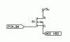
Need to shut down half my pcb to save power. Didn't really want to add another 5V regualtor since I already have one and its pretty large.

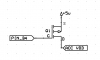
I have a car battery feed (10-15V) coming in and need to knock it all down to 4.75 - 5.10V. Then being able to source upto 250mA. My plan was to use my 5V regulator and then a mosfet to turn half the board off, but I forgot that fets cause a small voltage drop that would put my at about 4.3V. :oops:

I've been looking for the best way to do this. Maybe a transistor setup or an opamp a voltage follower mode ?

I'm not opposed to buying more components as long as they are small, cheap, and will help save power. Just not sure what the best approach is,

Any ideas ???
 
I don't know if this works all the time, but Ron H showed me you can get a 5V regulator to output ~5.7V by connecting a Si diode between the ground pin and the actual ground. That should just about make up for the FET drop assuming the diode current is right.
 
Overclock the regulator huh ? I really don't understand what would be going on there.

Sounds like it would lessen the life of my 5V regulator.

I'de buy a 5.2V but I need parts mouser has in stock NOW. And the regulator needs to able to handle automotive loads. So I'm pretty much stuck with 5.0.

I ruled out an opamp, its just not going to supply the current I need.

Maybe some sort of transistor deal where I can shut it off with an input from the micro,
 
Well, your 5.0V regulator places its output voltage relative to what it thinks is ground. If its ground pin is really at GND+0.7V due to a diode, it will place 5.7V on the output. More or less. All it needs is a series diode between the GND pin and ground.
 
Ah..... I see.

So then, if that works in my application... I'll need to pass my secondary circuit into a transistor, I get a ~.7V drop, but then I will also need to pass my primary circuit into some junction like a diode to get rid of that now pesky .7V.

If I put the micro to sleep and the total primary draw is 300uA... That diode is going to waste a good chunk of power no ?

I wonder if it is going to change voltages with temperature more then before the diode at the regulator?


I like the idea, I'm not sure its going to work tho. I need to get this whole thing down to as little power as possible.
 
Yes, that's correct. The actual volt drop on the diode will vary with both current and temperature, so your line and load regulation will suffer slightly.

The diode voltage drop will vary exponentially with the current exiting the GND pin. Additionally, its volt drop will fall about 2mV for every 1°C increase in temperature. So considering the extereme temperatures you can get in a car, that might be significant. What kind of 5V regulator did you have in mind?
 
I don't mind the temp drop as much as I do the increased used of power at the diode knocking the 5.7V down for the primary circuit.

I've have 1mA to work within. IF i can shut my circuit down to bare minimum I am looking at 900uA.

I'm thinking that .7 I'm going to be throwing away in the diode is going to screw up my 900uA no ???


The regulator is a ST-KF50, its not perfect but it meets all the criteria. Being instock at mouser is one of those requirments. I was hoping to order tommorow!

https://www.mouser.com/index.cfm?ha...uctid=210633&e_categoryid=260&e_pcodeid=51138
 
A mosfet has no foward voltage.It has a chanel resistance.This is the resistance betwen the pins when its saturated.I have mosfets that have this resistance of 0,008 Ohm and this is almost a wire.But you dont need that low. meaby like half a ohm.The less the better
 
Someone Electro said:
A mosfet has no foward voltage.It has a chanel resistance.This is the resistance betwen the pins when its saturated.I have mosfets that have this resistance of 0,008 ohm and this is almost a wire.But you dont need that low. meaby like half a ohm.The less the better
Adding to that: You need a P-channel MOSFET with Rds(on) specified at 4.5V. As Someone Electro said, there are many to choose from. Try irf.com or fairchildsemi.com, or some of the other MOSFET mfrs.
 
So...... If I have my secondary cicuit being driven @5V through a mosfet with .5ohm drop, and I draw 300mA from it, my voltage drop will be ???

I'm crappy at figuring this out but, its low.... like .015V no ?

If thats the case, that'll do!


So to calc that its just the original voltage - (resistance * amperage) ?


edit:
I read this data sheet:
https://www.electro-tech-online.com/custompdfs/2006/03/FDC6304P.pdf

I'm curious as to why they list all the values as negitive. As if everything is in respect to the source and not the drain ? But really the drain is there the feed is coming into the fet so why is it listed in the sources view ?

This transistor has an Ron of 1.1Max @ 4.5/.5A... It seems as voltage and amperage go up the Ron goes down. Is this true for Voltage AND Amperage or just Voltage ? Is there a way to determine the value @ 5V/.3A ? I looked at the graphs, but it didn't exactly tell me, looks like ~1ohm.
 
iso9001 said:
So...... If I have my secondary cicuit being driven @5V through a mosfet with .5ohm drop, and I draw 300mA from it, my voltage drop will be ???

I'm crappy at figuring this out but, its low.... like .015V no ?

If thats the case, that'll do!


So to calc that its just the original voltage - (resistance * amperage) ?
Yeah, except 0.5ohms *0.3A=150mV. Not a problem, though. It's easy to find a PMOS with Ron<0.05ohms.
 
Oh, yea my mistake. .150V Still fine.

So was I right about MOSFETs being measured to thier Source and thats why those values are almost all negitive ?

I included a quick diagram but I'm thinking its layed out of N-Channel all of a sudden. I've got 4 other project I'm working on and I know I've got to be making mistakes somwhere :)

I need to check and see if this is correct or not, also I need to figure out how I should bias this.... Or if I even need to ?
 

Attachments

  • untitled-1_345.gif
    untitled-1_345.gif
    1.4 KB · Views: 468
Close, but no cigar. See below. No biasing needed, if your logic input swings from zero to +5V.
And it does have to be P-channel.
 

Attachments

  • untitled-1_346.png
    untitled-1_346.png
    2.6 KB · Views: 454
Edit: I'm dumb just noiticed I used G instead of S.... sorry, hit the wrong key apparently.

Ok, I'll make the change.

I'm a little confused about the biasing tho. The last time I accidentely made a touch switch, but that was an N-Channel

But I understand getting a few stray electons to trigger then N-ch is probably easier then finding a close place to sink enough to fake a P-ch out,

I'll trust you and leave the biasing out for now. Just need to make sure I cut the power before I make the micro sleep.

Thanks Again Everyone!
 
iso9001 said:
Edit: I'm dumb just noiticed I used G instead of S.... sorry, hit the wrong key apparently.

Ok, I'll make the change.

I'm a little confused about the biasing tho. The last time I accidentely made a touch switch, but that was an N-Channel

But I understand getting a few stray electons to trigger then N-ch is probably easier then finding a close place to sink enough to fake a P-ch out,

I'll trust you and leave the biasing out for now. Just need to make sure I cut the power before I make the micro sleep.

Thanks Again Everyone!
I think you know this, but be aware that the PMOS is ON with the gate at zero volts (GND), and OFF with the gate at the same voltage as the source (+5V). As I pointed out above, be sure you use one that has Rds(on) specified at -4.5V or less (actually, I guess -2.7V is MORE than -4.5V, but I think you know what I mean).
 
Depending on your load's characteristics, sometimes NMOS will do fine. You unground that part of the circuit. But if it has outputs you want to go low then you don't want this.

Now be aware of the issues involved in gating off power to one part of a circuit. An op amp for example shouldn't have voltage on its input without power applied. Many chips have protection diodes that will cause current to flow from a normally high impedance input when the input voltage exceeds its power input (which is now at 0v, so basically any input over a 0.3v-0.7v threshold will cause current to flow).

Also the outputs of an unpowered section often appear as a floating to inputs on a powered section. Floating inputs are moderately bad. For the PIC for example once I powered down a section I just changed the inputs on the powered PIC which are hooked up to the unpowered device into outputs and then drove them to 0v.
 
I'll keep that in mind Oz,

There will only be IC's (transceivers and such) on the secondary side.

The only wires connecting them will be 3 SPI wires and 1 chip select wire each.

When the micro is asleep I think its recommended practice to drive all possible outputs low to conserve power. I never use those for input anyway, and somthing tells me the SPI pins have been designed with this in consideration. But I'll check,
 
iso9001 said:
The only wires connecting them will be 3 SPI wires and 1 chip select wire each.

When the micro is asleep I think its recommended practice to drive all possible outputs low to conserve power. I never use those for input anyway, and somthing tells me the SPI pins have been designed with this in consideration. But I'll check,

Well, keep in mind that it is probably a bad idea to power down one SPI device and then either drive an SDI or SDO signal to/from another device on that SPI bus. You should not put a voltage on the pins of a powered down device.

It is not required to drive outputs low to conserve power. Either high or low draws essentially no current and are usually equivalent. Still, if it's all the same, you might as well drive them all low as a rule. Just seems more logical. The thing to avoid is either a floating voltage on an input, or any voltage on an input which is not Vdd or Gnd. These nonboolean voltages can halfway turn on both the NMOS and PMOS of the pin's driver resulting in a small but real current directly from Vdd to Gnd inside the device. This is sometimes complicated to work around for pins which were designed to read an analog input and cannot simply be turned into an output and driven high/low because this would conflict with the external analog signal on that pin.
 
Good to know about the voltages on inputs.

But I don't really have a choice about the powered down SPI devices. No way around it.

I either draw 4mA in standby with everything powered, or I draw 900uA.

I'm thinking that someone thought of this when designing the SPI system. Maybe CS is hardwared internally to fets controling the SDI/SDO pins. They will probably just act as high impediance. Which as long as I have a powered device running should be OK (guessing here).

Actually, I just remembered when the other devices are unpowered I won't be using the spi anyway.

Still.... I wonder if I should force the SDI pin to output before I sleep... not certain but I think that my compiler's readSPI will automatically set to DI to input,

Guess I'll just have to build it and see :)
 
Status
Not open for further replies.

Latest threads

New Articles From Microcontroller Tips

Back
Top