Electro Tech is an online community (with over 170,000 members) who enjoy talking about and building electronic circuits, projects and gadgets. To participate you need to register. Registration is free. Click here to register now.
Welcome to our site! Electro Tech is an online community (with over 170,000 members) who enjoy talking about and building electronic circuits, projects and gadgets. To participate you need to register. Registration is free. Click here to register now.
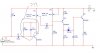
there's some part i didnt know what it does for the circuit, can anyone tell me what it functions as?? i've mark the parts with the pencil in the picture below... thanks for the help..
You should read up on transistor amplifiers. Personally I'm a bit rusty, but R4 biases Q1 into it's active region, and C2 makes Q1 into an low pass (inverting) amplifier. If you can simulate this, you should be able to sweep V2 over some frequency range and look at the gain of the first part of the circuit.
errr.. thanks for replying... but may i know what u mean by 'C2 makes Q1 into an low pass (inverting) amplifier'.. as i know, this part is function as amplifier. can u explain more details on that part? thanks...
errr.. thanks for replying... but may i know what u mean by 'C2 makes Q1 into an low pass (inverting) amplifier'.. as i know, this part is function as amplifier. can u explain more details on that part? thanks...
Both components give negative feedback (which reduces gain), the resistor gives DC negative feedback and makes the stage 'self biasing' and fairly independent of the transistor gain. The capacitor gives more feedback at higher frequencies, so reduces the gain at high frequencies - this is called a 'low pass' filter - although it's a fairly crude one.
thanks for the explanation...
i got something to ask again ^^
for this amplifier Q1, how can i calculate its gain?
and what voltage gain will i get for the output of transistor Q1?
what method or formula should i used?
more explanation is needed, thanks for the help...
thanks for the explanation...
i got something to ask again ^^
for this amplifier Q1, how can i calculate its gain?
and what voltage gain will i get for the output of transistor Q1?
what method or formula should i used?
It's difficult for these types of circuits, as far too many things affect it, if you want gain calculations use an opamp instead - where everything is nice and simple!.
hmm.....thanks for replying.
i'm currently working on this circuit and need to write report for the circuits but i lack of knowledge. so i hope someone can help me over it. what i need now is:
what theory should i used on that circuit?
and what formula or equation should i use?
since it is hard to calculate the gain, i think i will put in those formula inside my report only, but i hope someone can help me with the question above. thanks
The gain of Q1 is affected by the source resistance of the circuit feeding it, because the negative feedback through R4 and C2 form a voltage divider with the source resistance, and the negative feedback causes the input of the transistor to have a low resistance. The value of C1 determines how much low frequency signal reaches the transistor.
hmm.....thanks for replying.
i'm currently working on this circuit and need to write report for the circuits but i lack of knowledge. so i hope someone can help me over it. what i need now is:
what theory should i used on that circuit?
and what formula or equation should i use?
since it is hard to calculate the gain, i think i will put in those formula inside my report only, but i hope someone can help me with the question above. thanks
This site uses cookies to help personalise content, tailor your experience and to keep you logged in if you register.
By continuing to use this site, you are consenting to our use of cookies.