stevenmahoney
New Member
I am trying to repair an electronic ballast and do not understand some of its circuits. Can anyone help me?
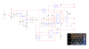
1) R4 suppose to regulate the brightness of HMI light. It looks like to me as a voltage divider (I am not even sure why transistors Q3 and Q4 were used, as they do not do anything). The voltage difference from highest to lowest at pin 3 of U2A when I rotate it is 1V. However, there is hardly any voltage on pin 2, so I am confused as to how that comparator should be operating. Also, the connection to Q9, Q10 transistors is not clear... Especially when resistor R19 is so low (.1 om).
2) U4 produces a square wave. I do not understand how it turned into an oscillator. Positive bias via capacitors C1 and C2? If so, how would it work?
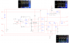
3) Pin 4 of U4 produces narrow square waves (pink on diagram). Is that suppose to be like this? U4 is a quad cmos NOR gate. Am I correct to assume that somehow the comparator U2A suppose to change the frequency or width of the signal on pin 4? This mechanism is also a mystery...
4) What is the purpose of transistors Q7 and Q8? How they suppose to work?
Basically I am trying to figure out how dimming works and fix it.
Any help (the more detailed the better) would be appreciated. Really want to get to the bottom of it...")
Steven
Detailed schematics with oscilloscope clippings are in the attached files.


1) R4 suppose to regulate the brightness of HMI light. It looks like to me as a voltage divider (I am not even sure why transistors Q3 and Q4 were used, as they do not do anything). The voltage difference from highest to lowest at pin 3 of U2A when I rotate it is 1V. However, there is hardly any voltage on pin 2, so I am confused as to how that comparator should be operating. Also, the connection to Q9, Q10 transistors is not clear... Especially when resistor R19 is so low (.1 om).
2) U4 produces a square wave. I do not understand how it turned into an oscillator. Positive bias via capacitors C1 and C2? If so, how would it work?
3) Pin 4 of U4 produces narrow square waves (pink on diagram). Is that suppose to be like this? U4 is a quad cmos NOR gate. Am I correct to assume that somehow the comparator U2A suppose to change the frequency or width of the signal on pin 4? This mechanism is also a mystery...
4) What is the purpose of transistors Q7 and Q8? How they suppose to work?
Basically I am trying to figure out how dimming works and fix it.
Any help (the more detailed the better) would be appreciated. Really want to get to the bottom of it...
Steven
Detailed schematics with oscilloscope clippings are in the attached files.
Attachments
Last edited:
