Continue to Site

Welcome to our site!

Electro Tech is an online community (with over 170,000 members) who enjoy talking about and building electronic circuits, projects and gadgets. To participate you need to register. Registration is free. Click here to register now.

  • Welcome to our site! Electro Tech is an online community (with over 170,000 members) who enjoy talking about and building electronic circuits, projects and gadgets. To participate you need to register. Registration is free. Click here to register now.

Need help to understand circuit!!!

Status
Not open for further replies.

pppopey

New Member
Hi everyone

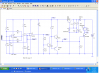
This following schematic is of a 24V DC motor speed control circuit that can handle a little bit over 10A.

Could anyone help me in the basic understanding of this circuit, how it works and what do the main components do.

It'll be a big help.

If you need anything else please let me know.

PS: In the schematic, getting rid of the jumper makes it 24V. IC = lm324, TR2 & TR3 = 9013, TR4 = 9012, TR1 = BC547, Zener = 10V, Mosfet = IRF3205
 

Attachments

  • fsjlf.jpg
    fsjlf.jpg
    68.2 KB · Views: 656
Last edited:
The first opamp is a triangle wave generator which feeds the second opamp setup as a comparator this part converts voltage from vr1 into a PWM signal (pulse widith modulation).
The three transistors following the second opamp form the driver to drive the gate of the mosfet.
The other transistors and diode(s) form a regulator and can be replaced by a common 3 terminal regulator chip such a the LM78xx series depending on the current demand of the motor.
I could have gotten greater in detail but the schematic is to small to see while I am typing in the comment box.
But that is basicaly it in a nutshell.

jer :)
 
That's a good explanation, geraldfryjr. I'll just add, in case the OP doesn't know, the purpose of the PWM or vairable duty-cycle produced by IC1 & IC2 is to effeciently provide variable drive for the motor. It's a common technique.
 
Its just a PWM circuit (common one) which drives a mosfet. IC1 produces a square wave at out put, here in circuit the triangular wave generated by the capacitor charging/discharging cycle is used for generating the triangular wave. the second op-amp will act as a comperator which will create the PWM output, for which the duty cycle is governed by the variable resistor. the TR2 act as a drover for the next push pull stage using TR3 and TR4. the amplified signal is given to the gate of the MOSFET which will correspondingly generate higher wattage PWM for the fan. the circuit using TR1 is a constant current source (i think) for the proper working of the IC.
 
TR1 is a voltage regulator whose voltage is set by the zener diode in the base.
 
Thankyou so much - geraldfryjr, BrownOut, magnatro, ronv for your detailed replies.

I am a second year electronic student and I am trying to build a motor speed control circuit for a 24V, 300W motor.

If it is not too much to ask for, as you guys have already provided me with such intense detail of the working of the circuit, I have the values of the components of the schematic, attached to this thread.

It is actually a schematic of a motor speed control for 12/24V motor with max current handling ability of upto 15A. Could you be able to guide me how to approach for calculating eg: the resistor values, what kind of output am I looking for out of IC1 and IC2. And biasing the transistors and mosfets, as these terms are still new to me.

I want to learn as much as I can about this schematic's working and its calculations for component values and component choice.

Thankyou so much!!!
 

Attachments

  • cct.jpg
    cct.jpg
    355.4 KB · Views: 310
Pwm

Here is a simulation of your PWM. Slight difference in components, but same functionality. See what questions it raises.
 

Attachments

  • pwm wave.PNG
    pwm wave.PNG
    75.4 KB · Views: 351
  • pwmw.PNG
    pwmw.PNG
    75.7 KB · Views: 214
I started a long post last night only to have to retype it,

You can breadboard that whole thing and verify every thing using a scope if you just want to understand how it works.
Except the FET as it needs to be on a heatsink and the proper gauge wires used to feed the motor for the amount of current that you are designing it for.
Or you can use any IRF XXX (510,z44,z42,640,740,840,540) and a smaller motor or lightbulb to verify its operation.
The regulator circuit is only for the opamp so you can use a LM7812 to save on parts count.

You can also get better performance and precision if you use a dedicated comparator chip for IC1-2 this is some thing that I would consider if you plan on controling such high currents.

It is your basic PWM circuit and I have built one before and I had alot of fun with it as it has endless uses.
I used mine for a basis for a Class D amplifier.

The other thing I did was to use the TL082 dual opamp to generate a precision triangle wave as I couldn't find a single stage circuit that was linear enough for my liking.
I used a 1/4 of LM339 but there are dual and single precision versions available as well.

Using a TTL buffer on the output to clean things up abit it worked flawlessly and even gave me an output exactly duplicating the input voltage.
My output voltage went from 0V to 5V
A sine wave was used as the input signal and the ouput running into a large inductor as a lowpass filter and there was no noticeable distrotion within its range even with a sqaure wave at various voltage levels as the input waveform.

Make sure that you use the diodes across the motor as the inductive kick of the motor could kill the FET if its voltage is not rated high enough.
My circuit was running somewhere in the 100khz to 200khz range.

I hope that helps you !

jer :)
 
Last edited:
Driving The FET was the hardest thing for me to figure out and the transistor driver in your circuit is what I had came up with as well and works great as you can't drive it directly from a TTl source very well as it does not turn the FET off completely or fast enough in most cases and I have burned up many of them because of this until I had figured it out.
So I wouldn't try starting off trying switch such high currents until you fully understand the how's and why's of each stage of this type of circuit.
Hmmmmmm.......I you have made me want to get my circuit back out and start messing with it again ! he,he


jer :)
 
lol thanks loads - geraldfryjr, i hope you do get your old circuit out :D... i am trying to build this circuit only, only problem is I cannot get the 9012 and 9013 transistors... or any other like those, would you be able to recommend any transistors specific to this or can i use any transistors?

by the way, i am trying to work out the frequency for the oscillator(IC/1), the frequency is set by the values of R4 and R2 someone told me... is that true? and if it is, what is the formula to set the frequency, if u know?!
 
I used common BJT's for the tranistors.
2N3904 and 2N3906 types that I got 15 in a pack at radio shack for $2.
Their numbers or not critical as they are just used for hard switching.

The formula for the frequency is " 1/(2RC) " as this is called an opamp relaxation oscillator.

https://www.electro-tech-online.com/custompdfs/2011/09/Exp_9_OP_Amps_v08.pdf

With the values shown in your diagram the frequency will be quite low,50k ohms and 100uf.

A .1uf capacitor with a 50k ohm resistor would give you a frequency of about 100Hz just to give you an idea.


jer :)
 
Last edited:
The other transistors and diode(s) form a regulator and can be replaced by a common 3 terminal regulator chip such a the LM78xx series depending on the current demand of the motor.
jer :)

Why do we need a voltage regulator around 10-12 volts in the circuit?
 
Basicaly to limit the gate drive voltage from exceding the maximum gate voltage or else it will damage the FET.
For the IRF3205 this voltage is +/- 20V and of course to provide a regulated source for the opamp as well as the gate driver transistors as any fluctuations of this voltage can also change how much the FET will conducted when it is on.
The voltage level on the gate determines how much current is allowed to flow through the FET.

Note fig 1,2,and 3

https://www.electro-tech-online.com/custompdfs/2011/10/irf3205.pdf
 
I have a concern. I got told that mosfet switches in khz range. my operating frequency is 100hz. 1/(2.2 * 50k*100uF) = 100hz.

Is this going to be the same as the mosfet switching frequency? If so, shouldn't it be in khz range for the mosfet to work properly dissipating less power?
 
Some FET's can even switch well into the Mhz range.

If your using a frequency of 50hz at say 50% duty cycle then your pulse will be 10ms.

By using the chart in fig.8 of the data sheet,
This shows that the maximum amount of current that the fet conduct at about say 24v is 10 amps for that single instant.
A little more than the maximum dc power maximum of 200 watts for the fet and the output voltage will be 12v (50% of 24v)
if you were to increase or frequency to 5khz then your pulse will be 100us at 50% dutycycle and the FET will be able to conduct 100 amps for that instant.

This is were it gets tricky and where the chart in figure 11 comes into play and is about my understanding is limited so I will read up on it some more and see if I can explain it better.

But I can say it like this,
The Fet is either on or it is off just like a switch and dissapates little heat when it is full on and none when it is off.
it is when it is operating in its linear range when it induces a resistance to the flow of current and has to dissapate more heat.
When it is full on its resistance is (RdsON) .008 ohms ( 8mohms) so it only has a drop of .8v at 100 amps.
It has to dissipate 80watts while it is flowing 100 amps at 23.2v across the load with a 24v supply for that 100us pulse.

I hope this gives you an idea as to why and how it works,
If any one can explain this in greater detail feel free to jump in on this as this is the best to my knowledge on this subject for now.

Here are some links that explain the switch mode action in greater detail,although this is more geared towards Class E RF operation Class D is also included as well as they are both switching amplifiers circuits.

https://www.electro-tech-online.com/threads/60w-rf-amplifier.120703/#post1006252

jer :)
 
Last edited:
Here is a simulation of your PWM. Slight difference in components, but same functionality. See what questions it raises.

ronv, is it possible if you can load the LTSpice schematic file? I am having some problem putting some components in the schematic.
 
Pwm

Here is the asc file for the PWM. The only problems you might have are with the 324 or the pot. They are the only imports that weren't in the original spice library. If you don't want to mess with trying to get the models you can replace the pot with 2 resistors and almost any op amp will work.
On the FET issue:
The FET is capable of switching much faster if you want it to, however the LM324 is not very fast so if you want to move the frequency up to say 20KHZ you should change it with a comparator as mentioned earlier. As to switching frequency Jer's answer is almost right. During the turn on and turn off time of the FET there will be a point of maximum power dissipated in the FET (If the load were resistive this would be the half way point). This power, which can be quite high, needs to be added to the steady state power when calculating the total power dissipation in the FET. Since this only occurs during switching the time is usually very short (nanoseconds) so it doesn't make much difference if the switching rate is low, but it can become important if the switching frequency gets high since it happens more often.
 

Attachments

  • comp pwm.asc
    5.9 KB · Views: 127
this is the schematic i made but i think i got the equivalent pot wrong.
 

Attachments

  • Draft1.asc
    5.1 KB · Views: 129
Status
Not open for further replies.

Latest threads

New Articles From Microcontroller Tips

Back
Top