Continue to Site

Welcome to our site!

Electro Tech is an online community (with over 170,000 members) who enjoy talking about and building electronic circuits, projects and gadgets. To participate you need to register. Registration is free. Click here to register now.

  • Welcome to our site! Electro Tech is an online community (with over 170,000 members) who enjoy talking about and building electronic circuits, projects and gadgets. To participate you need to register. Registration is free. Click here to register now.

Need help identifying unknown chip

Status
Not open for further replies.

Smartie

Member
Hey guys,

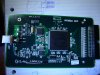
I have a FPGA based logic analyser that I'm trying to reverse engineer so I can load my own code onto it and add more memory.

While in the process of reverse engineer it, Most of the ICs have had their part number removed meaning I'm unable to identify what the IC is.

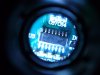
I've figured out two of four chips that are unknown, A FPGA (ep1c6q240 Altera Cyclone) and a Op-Amp (LM358). However I can't figure out the part number for this particular one.

I'm assuming it takes in a Serial signal but I do know that it outputs a voltage or analog signal as I can see it with my multi-metre when i change the threshold voltage in the software on my PC.

I have attached Images of the IC and of the logic analyser.
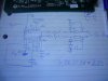
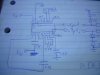
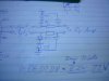
I did some tracing with my multi-metre and was able to draw out a simple schematic of the Chip.

I think the Chip could be a DAC and it does have the Texas Instruments logo on it, but I was unable to find a datasheet in the DAC section that fit with this Chip.

Any help would be greatly appreciated!!!

Cheers
Roman
 

Attachments

  • P1050018.JPG
    P1050018.JPG
    651.3 KB · Views: 207
  • P1050022.JPG
    P1050022.JPG
    509.9 KB · Views: 211
  • P1050025.JPG
    P1050025.JPG
    531 KB · Views: 174
  • P1050028.JPG
    P1050028.JPG
    672.1 KB · Views: 283
  • P1050026.JPG
    P1050026.JPG
    438.1 KB · Views: 171
Just a little update, the two traces connecting it to the FPGA can't be I²C as I²C requires pull-up resistors yet there are no resistors connected to the traces
 
Just a little update, the two traces connecting it to the FPGA can't be I²C as I²C requires pull-up resistors yet there are no resistors connected to the traces

It only really requires pullup resistors for multiple devices, and there's no reason they couldn't be internal to the FPGA.

But for simple communication between two chips there's no need (or reason) to use I2C anyway.
 
That is a valid point, however, there is a serial communication going on with this chip, maybe I²C, could even be UART...

I'm sure its a DAC but I can't find any datasheet to match the pin layout... well the voltage output pins don't match. I'm still looking through them
 
Diver300 is spot on, with 4 SMD caps there, and how they are connected to the SOIC16 chip, looks like a level shifter/charge pump '232. Possibly to analyze RS232 signal levels? I know that the original cyclone series (like the second and third) didn't have 5v tolerant IO's, let alone +/-12v... so maybe thats why..or even to power the LM358 with the output from the charge pumps (nice trick on dev boards that).
 
Diver300 is spot on, with 4 SMD caps there, and how they are connected to the SOIC16 chip, looks like a level shifter/charge pump '232. Possibly to analyze RS232 signal levels? I know that the original cyclone series (like the second and third) didn't have 5v tolerant IO's, let alone +/-12v... so maybe thats why..or even to power the LM358 with the output from the charge pumps (nice trick on dev boards that).

Well the LM358 is powered by the USB and there are two traces going from this chip to the non-inverting inputs of the Op-Amp
 
Well,I was just speculating as to its purpose, because I don't see a DSUB RS232 connector on that board. But as driver300 stated, its a max232 equivilent:

**broken link removed**

As you can see fomr that pinout, the power/gnd connections and the caps are identical to your drawing. Asto the opamps function? dunno :)
 
Wow, I really did not think that a Level shifter was being used. Maybe it's given a PWM signal and it smoothed with capacitors?
The purpose of this circuit is to set a threshold voltage to the input on the logic analyser. I'll draw up a schematic and post it here shortly
 
Ok, Here's the schematic of it made in Eagle.
It is weird that a max232 is being used though.

Edit: Just to note, There are inductors being used on the outputs of the op-amps, maybe they are smoothing out the output. I'll find out once I've got hold of a oscilloscope.
 

Attachments

  • Threshold Voltage Adjust Schematic.png
    Threshold Voltage Adjust Schematic.png
    13.2 KB · Views: 204
Last edited:
Status
Not open for further replies.

New Articles From Microcontroller Tips

Back
Top