Continue to Site

Welcome to our site!

Electro Tech is an online community (with over 170,000 members) who enjoy talking about and building electronic circuits, projects and gadgets. To participate you need to register. Registration is free. Click here to register now.

  • Welcome to our site! Electro Tech is an online community (with over 170,000 members) who enjoy talking about and building electronic circuits, projects and gadgets. To participate you need to register. Registration is free. Click here to register now.

Need Help Finding An On-Off Surface Mount Switch that Is Large Enough To...

Status
Not open for further replies.

rs14smith

Member
Hi all,

I need to find a surface mountable On-Off switch that can be mounted near the very edge of my PCB and once the PCB is placed in an enclosure and holes are cut, I can easily access the switch. Similar to how people have mini USB ports that stick on the side of the PCB and that port can be accessed easily externally once a hole is cut for it on a box enclosure.

I will be using Eagle to place the piece, so it would be great if the part is in the library, but if not I guess I can figure out a workaround.

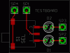
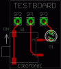
I need to replace the on-off switch on this PCB:
(At the top near the GND port)
 
Yeah, I think I found the one I will go with, the next hard part is creating this device in Eagle since there does not seem to be a library that has it already: http://search.digikey.com/us/en/products/ES02MSABE/CKN1813CT-ND/717131 The switch needs to be small, but still capable of being large enough to make it not too hard to switch it on and off from outside the box.
 
Hi rs14,

I tried to create a package for your switch. I used the datasheet provided at Digikey and referred to page6 for the SMT footprint.

There are some slight discrepances in dimensional values converting from inches to mm. I used the inch based numbers up to 1/1000" accuracy.

Please print the footprint and check if it matches the switch you are using. I will then finish the design for an entire Eagle device.

Attached is the zip file ES01.zip.

Boncuk
 

Attachments

  • ES01.gif
    ES01.gif
    3.6 KB · Views: 286
  • ES01.zip
    1,010 bytes · Views: 234
Hi rs14,

I tried to create a package for your switch. I used the datasheet provided at Digikey and referred to page6 for the SMT footprint.

There are some slight discrepances in dimensional values converting from inches to mm. I used the inch based numbers up to 1/1000" accuracy.

Please print the footprint and check if it matches the switch you are using. I will then finish the design for an entire Eagle device.

Attached is the zip file ES01.zip.

Boncuk

Yeah I actually watched a tutorial on how to make the part on Eagle, and from your image, ours look very similar but I will add yours to my library just to see how close we got. Thanks for going out your way to do that!
 
Last edited:
Hi rs14,

here is the entire device for your switch. I guess I'll have use for it as well since it is really small.

I connected the solder pads at the front end to pins. Connecting those pins to circuit ground might be useful when switching high frequencies, since the switch seems to be completely metal encapsuled.

When dropping the switch onto a schematic activate the pins layer. You'll see two unnamed pins seeming to go nowhere. They are in fact connected to those mentioned solder pads.

You will see the package outline as posted if layer51 is activated. After deactivating it there won't be any annoying contour lines across the SMD pads. (Layer51 is never used in board houses.)

The test board connects OK.

I like Tennessee people. They used to fire their rifles at our planes after too many of them had been caught brewing moonshine in the woods.

We made nice infrared "movies" of the distilleries. ;)

Regards

Boncuk
 

Attachments

  • ES01.zip
    1.4 KB · Views: 238
  • ES01.gif
    ES01.gif
    6.9 KB · Views: 296
  • ES01-BRD.gif
    ES01-BRD.gif
    16.4 KB · Views: 283
Last edited:
Hi rs14,

here is the entire device for your switch. I guess I'll have use for it as well since it is really small.

I connected the solder pads at the front end to pins. Connecting those pins to circuit ground might be useful when switching high frequencies, since the switch seems to be completely metal encapsuled.

When dropping the switch onto a schematic activate the pins layer. You'll see two unnamed pins seeming to go nowhere. They are in fact connected to those mentioned solder pads.

You will see the package outline as posted if layer51 is activated. After deactivating it there won't be any annoying contour lines across the SMD pads. (Layer51 is never used in board houses.)

The test board connects OK.

I like Tennessee people. They used to fire their rifles at our planes after too many of them had been caught brewing moonshine in the woods.

We made nice infrared "movies" of the distilleries. ;)

Regards

Boncuk

I noticed from your schematic file that you are using the wrong symbol type I think. You have pins 1, 2, and 3, but for the ES02MSABE, they only use pins 1 and 3 in the schematic symbol. I'm still new to part making so if I'm wrong, let me know why they have it drawn like that in the schematic. I have attached the image for your convenience.
 

Attachments

  • Screen Shot 2012-01-14 at 10.24.02 PM.png
    Screen Shot 2012-01-14 at 10.24.02 PM.png
    27.5 KB · Views: 264
  • Screen Shot 2012-01-14 at 10.26.36 PM.png
    Screen Shot 2012-01-14 at 10.26.36 PM.png
    8 KB · Views: 276
Last edited:
Oh nevermind, I see now. You did not know which one I was making from the 3 types, but that is fine. I am using the ES02, but I should be able to edit your library file to tweak the pins and the schematic drawing. You did an awesome job on the board drawing!
 
Oh nevermind, I see now. You did not know which one I was making from the 3 types, but that is fine. I am using the ES02, but I should be able to edit your library file to tweak the pins and the schematic drawing. You did an awesome job on the board drawing!

Hi rs14,

I assumed you will use a SPDT for your project, which provides the option to position the switch either on the LH or RH side of the PCB to power up the circuit by pushing the switch (moving the slider upwards).

According to the pad layout the SPDT symbol won't fit since the SPST switch closes terminals 1 and 3.

I will add that switch in the library and post it here.

Removing one solder pad and adding a new symbol is a matter of minutes.

Boncuk
 
Last edited:
Hi rs14,

I assumed you will use a SPDT for your project, which provides the option to position the switch either on the LH or RH side of the PCB to power up the circuit by pushing the switch (moving the slider upwards).

According to the pad layout the SPDT symbol won't fit since the SPST switch closes terminals 1 and 3.

I will add that switch in the library and post it here.

Removing one solder pad and adding a new symbol is a matter of minutes.

Boncuk

Yeah for my application, I just needed an On-Off switch. I think the other one's are On-On switches.
 
Last edited:
Yeah for my application, I just needed an On-Off switch. I think the other one's are On-On switches.

Not quite. The SPDT switch is a three position switch with the center position OFF.

Anyway, here is a testboard and the revised zip file. Have fun!

Boncuk
 

Attachments

  • ES02.gif
    ES02.gif
    13.1 KB · Views: 294
  • ES01.zip
    1.7 KB · Views: 232
Status
Not open for further replies.

Latest threads

New Articles From Microcontroller Tips

Back
Top