partick_sun
New Member
Dear All,
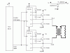
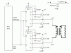
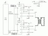
First, thanks for reading my writing. I have design a full-bridge DC-AC inverter with 12Vdc input voltage and 220Vac output voltage. In my inverter, I use a 8051 micro-controller to give the "sine" PMW singnal. Since I am designing the full bridge version, the 8051 uP gives complementary signals. I choose four "Ix" (I don't know can I state the brand name or not, so I hope all of you will know which one it is) Power-NMOSFETs to be the full-bridge stage. In order to drive those "Ix" NMOSFET, the "Ix2110" driver is used. This gate driver use the boostrap method to drive the high-side NMOSFET.
Up to now, at least myself, think the circuit is okay
However, when I connect the the primary side of the transformer to my full-bridge output, with the secondary side connected with a pure resistive loading, it should be okay to measure the step-up "sine" PWM signal at the secondary side (I think). Unfortunately, I cannot measure anything (all are noise). More worse is that, after several seconds, the "Ix2110" driver "dead" in a way I don't know what is happening.
So, any one can help me?
If you want more information, I am willing to supply them
Thansk alot
Patrick