Tickled_Pink
New Member
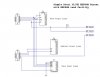
After much design and redesign I *think* I've finally come up with a schematic that'll work.
This is a simple EEPROM burner for the Atari XL/XE 8-bit computer. It connects to the joystick ports. The difficulty I had with this was due to the limited number of I/O pins available (8 - can't wait until a friend finally sends me the Atari 400 he promised me ... it'll make project work so much easier). I've noticed that a lot of simple EEPROM/EPROM programmer projects on the net are write only with no facility to read the memory back afterwards for verifying the data and so forth. That was something I wanted to incorporate.
Anyway, here's some technical info. Hopefully someone will be able to pick out some problems with the design.
The Atari 8-bit's joystick ports, from my recollection of past magazine articles, provides around 500mA. However, by the time it travels along the wire to the project board it seems to be a lot less. I blew up an LED when I connected it directly to the +5v and GND lines on one of the ports. But when I connect an LED to the port through the cable and the board, the light from the LED is much dimmer and I've yet to destroy one that way - even without a current limiting resistor.
The design of the project itself is based around the 4094 8-stage shift/store register with 3 stage outputs (I'll be specifically using the MC14094), the 4040 binary ripple counter, and the 74166 (I think I have the HC or HCT and not the LS, however) parallel in/serial out shift register.
The 4094 is used to output the data to be written to the EEPROM. The 4040 is used to select each memory address to read from/write to, and the 74166 is used to read the data back from the EEPROM.
The principles of operation are as follows:
Writing to the device
1. Clear U4 with the Master Reset input. This sets the counter to the first memory location.
2a. Enable U1. This also has the function of setting the EEPROM to 'Write Enable' mode.
2b. Send serial data to U1 from J1. This will write the data to the EEPROM.
2c. Disable U1 (just in case).
2d. Increment U4. Goto 2a and repeat process as often as necessary.
Reading from device
1. Disable U1 in case it hasn't already been done. This will also put the EEPROM into 'Output Enable' mode.
2. Clear U4.
3a. Load parallel data into U2 by setting 'PE' low.
3b. Load 8 bits of data into U2 and read the output from Q7. This is the data from the EEPROM.
3c. Increment U4. Goto 3a and repeat process as often as necessary.
Now, for the schematic ...

")
