Continue to Site

Welcome to our site!

Electro Tech is an online community (with over 170,000 members) who enjoy talking about and building electronic circuits, projects and gadgets. To participate you need to register. Registration is free. Click here to register now.

  • Welcome to our site! Electro Tech is an online community (with over 170,000 members) who enjoy talking about and building electronic circuits, projects and gadgets. To participate you need to register. Registration is free. Click here to register now.

multiplexing using 74hc595

Status
Not open for further replies.

tcop

New Member
Hi,
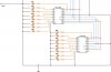
I use two 74hc595 shift registers to drive 6 - 7 segment displays (common cathode) using the multiplexing technick. The first drives the anodes of the seven segment displays and the second drives the cathodes. I ve done it succcesfully but i faced the following problem. I dedicate RA1 pin of my 16f628 for producing the clock pulses but when i shared it to both the s/r one of them did not function properly so to resolve it i used an extra pin and a second clock sending exactly the same pulses to the second s/r. It seemed that i got a noise problem or something and havent yet found a solution apart from using an extra pin. Any ideas how to share the same clock to both the shift registers?
 
Last edited:
Why are you bothering with bit banging serial to the chips when the 16F628A has a USART on chip that will serve as an SPI interface?

It also appears that those chips don't have a chip select (CS) pin so I don't think you'll be able to run them both on the same clock line.
 
Isn't that how they daisy-chain 74HC595's Jon?

For some reason I was thinking that the chip would need a CS line so that the one that isn't having data transmitted to it wouldn't listen to the clock pulse.
 
I am not doing something fancy at all. Instead of using one 74hc595 for each 7 seg display (6 in total) , i multiplex them using 2 x 74ch595. On the pic side, i have 2 data lines. One for the segments (anodes) of all the displays and one for the cathodes. (note that Dig1 SegA, Dig2 SegA,... Dig6 SegA are joined together and so are all the segments of all the displays).
To make the long story short on the pic side... i have 2 data pins , 2 pins for the shift register clock pulse and 2 pins for the storage register clock pulse (6 pins in total). The problem is that when i try to share the clock pins to the two 74hc595, the circuit does not work properly but it should since these pins carry exactly the some pulses, only the data are different.
It has to be a noise problem...but how can i solve it?
 
sorry but i haven made a schematic so far. I made one only for the displays so as to create the pcb.
 
hi tcop,
A circuit digram is worth a thousand words of text, any chance of posting a circuit diagram.??:)
 
well yes i but i need some time...
i dont think it will be of any help though?
It is a simple thing and it possibly has to do with noise. There must be a easy way out.
 
well yes i but i need some time...
i dont think it will be of any help though?
It is a simple thing and it possibly has to do with noise. There must be a easy way out.

hi,
Its wise to start with a simple circuit diagram, before you start building the circuit.

It may be simple thing that you have done wrong, a circuit diagram that we all could use as a point of reference would be helpful in debugging your project.
 
well yes i but i need some time...
i dont think it will be of any help though?
It is a simple thing and it possibly has to do with noise. There must be a easy way out.
Why not just use the two '595's in a standard daisy chain configuration? You have just one data, clock, and latch line. Be sure to clock out 16 bits each time, and pad with zeros where necessary.

This has got to be a pretty dim display, unless transistor/mosfets are supply the common supply.
 
Yeap, that's the way out...
by the way, do you think i should use bypass capacitors between V+ and GND?
 
Here you some thing to start with
 

Attachments

  • shift_register_07_lrg.jpg
    shift_register_07_lrg.jpg
    77.3 KB · Views: 531
Yeap, that's the way out...
by the way, do you think i should use bypass capacitors between V+ and GND?

hi tcop,
Not to sound a smartie, but if you had posted a diagram we could have spotted that PDQ...:rolleyes:
 
Thanks guys for the info but my circuit is already working and succesfully driving 6 x 7 seg displays...meaninig 42 leds. :)
The thing with the clock was noise as i suspected, but i altered the topology to daisy chain as nickelflippr proposed so i saved two more pins from my pic (SH_CP and Data for the second 595). Now i send 16bit data from one pin instead of 8bits data from two pins. So my project finally uses 3 pins from the 16F628 and drives 42 leds but can go up to 64.
When i'll find some time to make the shematic in eagle I'll upload it here....but the thing here is not the schem which is easy to do but the asm code.
 
Last edited:
Status
Not open for further replies.

Latest threads

New Articles From Microcontroller Tips

Back
Top