Continue to Site

Welcome to our site!

Electro Tech is an online community (with over 170,000 members) who enjoy talking about and building electronic circuits, projects and gadgets. To participate you need to register. Registration is free. Click here to register now.

  • Welcome to our site! Electro Tech is an online community (with over 170,000 members) who enjoy talking about and building electronic circuits, projects and gadgets. To participate you need to register. Registration is free. Click here to register now.

Mosfet Delay question

Status
Not open for further replies.
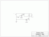
Within the attached schematic, I've got two mosfets set up in order to give a motor power when it's triggered, and a loop specifically meant to create a form of active breaking when the trigger is released. Now, here's my question: would it be ok to run everything within it's current configuration, or is it absolutely necessary to have some sort of delay between when one mosfet and another allows current to flow?
 

Attachments

  • mosfet switch.jpg
    mosfet switch.jpg
    39 KB · Views: 379
Doesn't matter with this circuit. Q2 will always be on, as its source is at 8.4v and the gate cannot go higher than 4.5V. Vgs will be -3.9V when you think it should have been off.

But if you do get the voltages right, yes break before make is a good idea. Otherwise the 8.4V would have a direct path to 0V. The current spike would be momentary but the only limit for the current would depend on how poor the wiring is (worse wiring = less damage).
 
The wiring within this circuit is planned to be at as low resistance as is possible to ensure the motor is driven with as much current as it requires. (something between 20-30amps)


So, say the regulator is removed, and the 555timer is inserted. My thought for this is everything is off before the triggerswitch is pushed and the timer is reset. Once the trigger is engaged, the motor spins as it should. Once the trigger is released, Q1 begins switching it's state, the mono-stable timer is triggered, and it's initial current flowing from the output pin is spent charging C5. once C5 is nearing 67%, the signal inverter is powered, allowing Q2 to change states (after Q1 has changed it's state), creating a resistance for the already spinning motor until it comes to a hault, at which point the timer will have completed it's cycle.

any thoughts, major errors, comments, suggestions?


This here is a similar circuit to one kchriste had helped me develop in a much earlier thread (when looking at the FET's), but all of the logic has been removed/replaced with the timer.


Schematic is attached below:
 

Attachments

  • mosfet switch.jpg
    mosfet switch.jpg
    60.6 KB · Views: 373
Sorry, I don't really understand what you're trying to do.

Do you want to make it so you press a button and it triggers and remains triggered until the power is removed?

It's possible to make a bistable with a couple of MOSFETs.
 
My goal here is for the motor to be powered when the triggerswitch is pushed, and for it to stop suddenly when the trigger is released. However, as mneary had mentioned, I do not want both mosfets to be conducting current, causing a straight line from Vs+ to 0V. Q1 is used to power the motor, and Q2 is used for the active breaking function. C5 is used to create a small delay between when Q1 stops conducting current (it is my assumption from its datasheet that it takes about 10ns to do this) and when Q2 begins conducting current. the 555 timer is used to shut off Q2 once the motor has stopped spinning completely.
 
Last edited:
My bad, the previous schematic had numerous errors, including me mixing up the N and P gates. Hopefully that clears up some of the confusion.
 

Attachments

  • mosfet switch.jpg
    mosfet switch.jpg
    60.6 KB · Views: 421
So, I've been working for quite a while on this circuit within a seperate thread, but seeing as where it sits, my question now pertains a-bit more to the title of this thread.

Within the new attached schematic, I've ditched the 555 timer for capacitor C2. In this case, when the trigger-switch is pushed, both capacitors in this design are meant to be shorted as the N-channel MOSFET is on. Once the trigger-switch is released, the initial current flowing "through" C2 is meant to begin charging C3, causing the delay as the N-channel MOSFET switches. Once C3 is charged (well, at least what it can be at with R4 there), C2 should still be charging, thus turning the P-channel MOSFET on after that delay. When C2 is fully charged, the P-channel MOSFET should be off.

What I'm asking now are these two things: Does the thought process for for this circuit seem alright, and are there any grave mistakes I have made? (as one could probably tell from the above schematics, I am very good at doing this)

Thankyou again everyone for your input!
 

Attachments

  • mosfet switch.jpg
    mosfet switch.jpg
    34.7 KB · Views: 217
Shoot thru timing

Try this one. The turn off is quick the turn on is slower for both fets. It uses the FET gate capacitance to set the timing.
 

Attachments

  • mtr. dr..GIF
    mtr. dr..GIF
    19.1 KB · Views: 214
Status
Not open for further replies.

Latest threads

New Articles From Microcontroller Tips

Back
Top