Continue to Site

Welcome to our site!

Electro Tech is an online community (with over 170,000 members) who enjoy talking about and building electronic circuits, projects and gadgets. To participate you need to register. Registration is free. Click here to register now.

  • Welcome to our site! Electro Tech is an online community (with over 170,000 members) who enjoy talking about and building electronic circuits, projects and gadgets. To participate you need to register. Registration is free. Click here to register now.
Status
Not open for further replies.

GiacomoPascon

New Member
Hi to all.
A few days ago, I started thinking to build on my own, a linear power supply able to output 30V 10 A.
I chose to use the L200 IC, because I've got some of them and I want to use some components recovered from old boards.
I started making the schematic following the application note pdf and things went smoothly until I started wondering how to adjust the current output, with a potentiometer.
I saw some examples in the PDF but I can't understand how that circuits works.
Can you suggest me a way to make an adjustable current limiting? (schematic is attached to the post)

Thanks in advance,
Giacomo.
 

Attachments

  • Schematic_L200 PowerSupply_2021-04-08.pdf
    34.6 KB · Views: 460
The L200 is a 2A regulator. However you want 10A output current. There is circuitry inside the L200 that regulates the maximum output current according to the voltage between pins 5 and 2. If this voltage gets higher than 2V, it starts to restrict the output current. This is where Q1 and Q2 come in... If the voltage across R1 is higher than 0.65 it starts to turn on Q1 and Q2 and these transistors bypass the regulator and provide most of the output current. This happens at currents (through R1) of greater than 30mA, so if your load current is higher than 30mA, Q1 and Q2 provide the current. If the voltage across R3 is higher than 2V, the L200 stops providing current. This limits the current flowing into pin 1 and thus limits the voltage drop across R1, so the output current is limited

FIG 23 in the datasheet shows a way of getting adjustable current.

You could use a variable 0.045 Ohm resistor (but you cannot buy these) so FIG 23 amplifies this voltage enabling you to use a higher value variable resistor. I dont agree with the current limit numbers specified in FIG 23 and need to look more into this
 
... with the circuit you provided, C4 is connected wrong. It should be connected to GND and not the top of R2. You'll get all sorts of stability problems if you connect it to the top of R2. I also worry about the heat dissipation in Q1 and Q2. These need to be big and mounted on a heatsink... and even then this might not stop them over heating
 
The L200 is a 2A regulator. However you want 10A output current. There is circuitry inside the L200 that regulates the maximum output current according to the voltage between pins 5 and 2. If this voltage gets higher than 2V, it starts to restrict the output current. This is where Q1 and Q2 come in... If the voltage across R1 is higher than 0.65 it starts to turn on Q1 and Q2 and these transistors bypass the regulator and provide most of the output current. This happens at currents (through R1) of greater than 30mA, so if your load current is higher than 30mA, Q1 and Q2 provide the current. If the voltage across R3 is higher than 2V, the L200 stops providing current. This limits the current flowing into pin 1 and thus limits the voltage drop across R1, so the output current is limited

FIG 23 in the datasheet shows a way of getting adjustable current.

You could use a variable 0.045 Ohm resistor (but you cannot buy these) so FIG 23 amplifies this voltage enabling you to use a higher value variable resistor. I dont agree with the current limit numbers specified in FIG 23 and need to look more into this

Hi Simon, thanks for your quick reply.
Using the formulas found on the pdf, I set the current to the regulator at about 100mA. At this current R1 should have a voltage of 1.5v across it, to turn on the PNP transistors (they are Darlington).
Moreover I read that the voltage between pin 2 and pin 5 needs to be at least 0.45v, so I have to redo the calculations for R3 to have 2V across it (at 10A), right?

... with the circuit you provided, C4 is connected wrong. It should be connected to GND and not the top of R2. You'll get all sorts of stability problems if you connect it to the top of R2. I also worry about the heat dissipation in Q1 and Q2. These need to be big and mounted on a heatsink... and even then this might not stop them over heating
I made a mistake in the schematic, Now I should have correct it.
Talking about the transistor, I put them on a very big heatsink, but if they overheat, I can add another in parallel without a problem. Each of them support 8 amps continuos.

Thanks again,
Giacomo.
 

Attachments

  • SchematicV2.pdf
    34.6 KB · Views: 345
You need emitter resistors in the power transistor emitters, to ensure equal load sharing - other wise one will get too hot and die.

I'm also dubious about heat dissipation in the output transistors, and concerned what you consider a "very big heatsink", it's going to have to dissipate a LOT of heat at high current and low voltage.

C1 and C2 seem a bit puny as well.
 
You need emitter resistors in the power transistor emitters, to ensure equal load sharing - other wise one will get too hot and die.
Thanks for the tip, do you know how to calculate the values? I'm new in electronics.

I'm also dubious about heat dissipation in the output transistors, and concerned what you consider a "very big heatsink", it's going to have to dissipate a LOT of heat at high current and low voltage.

C1 and C2 seem a bit puny as well.
Maybe I should add a 3rd transistor...
About the Capacitors, I'll have no problem adding more capacity if needed.
 
Thanks for the tip, do you know how to calculate the values? I'm new in electronics.

Just a matter of getting the transistors to share the current - something like 0.22 ohm 2.5W wirewounds should be fine, and a standard value.

Maybe I should add a 3rd transistor...

Bear in mind adding extra transistors splits the heat between the transistors, but you've still got the same total amount of heat in the heatsink.

Have you got a picture (or a link) of the kind of heatsink you're thinking of using?.
 
Just a matter of getting the transistors to share the current - something like 0.22 ohm 2.5W wirewounds should be fine, and a standard value.
I've added them on the schematic.

Have you got a picture (or a link) of the kind of heatsink you're thinking of using?.

I'm going to use those 3 heatsinks:

IMG_20210408_212554.jpg
 

Attachments

  • SchematicV3.pdf
    36.6 KB · Views: 285
Plosses = (Vin - VOUT)/Iout
5V 10A out ->250W losses
go for step down switching power supply
 
Plosses = (Vin - VOUT)/Iout
5V 10A out ->250W losses
go for step down switching power supply
That's another good idea, but I've got a bunch of components that I want to use and I thought that building a linear power supply was a way to learn something new and reuse some components laying in the drawers.
 
That's another good idea, but I've got a bunch of components that I want to use and I thought that building a linear power supply was a way to learn something new and reuse some components laying in the drawers.
I would reccomend you to go for step down PS. You will need those BJT transistors for smoothing ripple.
There will be constant voltage drop.
Also your PS will be much smaller. There wont be need for big heatsink... and it will be propably fanless..
 
Just to pick up on the Darlington comment, your transistors are not connected as a Darlington pair. With a Darlington, the emitter of one feeds into the base of the other so you get 1.3V drop across the total base emitter junction. Yours are connected in parallel, so the drop across R1 will only be one VBE.

Regarding your comment
Moreover I read that the voltage between pin 2 and pin 5 needs to be at least 0.45v
, there is a comparator connected between these 2 pins, so nothing happens until this voltage reaches 0.45V, then the comparator kicks in and limits the output current. Increasing this resistor reduces the trip current, thus providing variability in the output current
 
Just to pick up on the Darlington comment, your transistors are not connected as a Darlington pair. With a Darlington, the emitter of one feeds into the base of the other so you get 1.3V drop across the total base emitter junction. Yours are connected in parallel, so the drop across R1 will only be one VBE.

Regarding your comment , there is a comparator connected between these 2 pins, so nothing happens until this voltage reaches 0.45V, then the comparator kicks in and limits the output current. Increasing this resistor reduces the trip current, thus providing variability in the output current
They are 2 darlington transistor, according to the datasheet.
Thanks for the explanation about the comparator, now I understand how it works.
 
I would reccomend you to go for step down PS. You will need those BJT transistors for smoothing ripple.
There will be constant voltage drop.
Also your PS will be much smaller. There wont be need for big heatsink... and it will be propably fanless..
I think I'll go with a switching, can you suggest me a design to start?
 
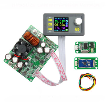
There are some nice cheap modules available from China, which will exceed what you can build - such as this one:

But he will skip learning process. If you wanna buy it, reverse engineer it than.
 
Last edited:
Status
Not open for further replies.

Latest threads

New Articles From Microcontroller Tips

Back
Top