Continue to Site

Welcome to our site!

Electro Tech is an online community (with over 170,000 members) who enjoy talking about and building electronic circuits, projects and gadgets. To participate you need to register. Registration is free. Click here to register now.

  • Welcome to our site! Electro Tech is an online community (with over 170,000 members) who enjoy talking about and building electronic circuits, projects and gadgets. To participate you need to register. Registration is free. Click here to register now.

Junebug Assembly Tips

Status
Not open for further replies.

Krumlink

New Member
For anybody almost done with their Junebug programmer or about to get one, I have a few important pointers for you. PS Bill: Check over your Assembly manual :D

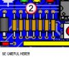
The attached images are ones that I think that you may be confused with. One that You may overlook is R11 and R12, they go under the 18F2550 and are 100 ohm resistors.

R7 is a 100k resistor

Watch the MOSFET Pin out

The 2N3904 is substitutable with a 2N2222A
The 2N3906 is substitutable with a 2N2907A

I will keep this updated as I go. Also, watch how you put in those switches!
 

Attachments

  • R7.JPG
    R7.JPG
    8.1 KB · Views: 353
  • 1.JPG
    1.JPG
    10.6 KB · Views: 377
  • MOSFETS.JPG
    MOSFETS.JPG
    4.1 KB · Views: 341
  • R11 AND R12.JPG
    R11 AND R12.JPG
    7.2 KB · Views: 338
Very nice, and yes those transistors will work. The tricky ones are the FETs but both are optional (they allow VPP before VDD programming and shorted target VDD testing)
I'm working on the manual a wee bit everyday.
I don't think the switches will fit in the wrong way, they're rectangular.
The ferrite bead is recommended but you can use a wire link if you don't have one.
And you can stand little 1/8 watt resistors where the SIPs go.
 
Last edited:
blueroomelectronics said:
you can stand little 1/8 watt resistors where the SIPs go.

OR, you could stand up some 1/4 watts like I am going to.
 
I am going to get the rest of the parts very soon, I really would like to use this, as well as my inchworm+. That one C class will love a couple of these :D

The next idea for a kit should be some kind of robot kit programmer, besides your mongoose. Is that even available yet?
 
My Breakout board, that I was thinking of. Its under robotics. Maybe you or 3v0 could help me set up one that uses a 16F88. It would be really cool (further down the road, but still applicable).
 
As a substitute for a ferrite bead, you can also run a wire through a small toroid, which is what I did.
 
I am building the JuneBug in 3 steps.
1. Get the programmer's processor working/talking/USB-connected (done)
2. Add the analog parts (transistors etc) to finish the programmer
3. The tutor.

I built the processor section (1) of the JuneBug programmer and have it working. Had a bit of difficulty with the unrecognized USB device error. It worked after I changed C6 to a .22uf ceramic cap. The cap that did not work was Mylar. Could have been a defective part. .22uF is within the range that Bill indicated.

The USB software driver is a non issue with the PK2. It uses standard XP supplied drivers.

You need to program the PIC18F2550 processor with another programmer such as the inchworm. The procedure can be done on a protoboard with the inchworm connected to the 18F2550. You do not need a crystal but it is a good idea to use a .1uF bypass cap between pwr and gnd.

Download the ziped hex file PICkit 2 Firmware V2.10. (if you are reading this much later then NOV 07 check for an updated version **broken link removed**).

Unzip the file and place the file PK2V021000.hex in a location that you can easily find. ie: C:\abc\PK2V021000.hex

Start MPLAB. You will not be using a project.

Configure>Select_Device> PIC18F2550

File>Import ... then browse to C:\abc\PK2V021000.hex and click on it.

You do not need to set the fuse/configuration setting because they are included in the hex file.

Programmer>Select_Programmer>MPLAB_ICD2

Programmer>Connect

Programmer>Program

That should do it. If anyone sees an error in this I will be glad to edit this post.

Good luck.
 
Last edited:
CUSB 220nf is the minimum recommend PIC18F2550 datasheet pg 376.

Glad you got the boards.

Here's the Junebug "Hello World"
Code:
 ;*** WDT reset toggles RA7 
   list     p=18F1320
   include <p18F1320.inc>
   CONFIG   OSC=INTIO2, LVP=OFF, DEBUG = ON
   CONFIG   WDT=ON, WDTPS=128
   org      0
   movlw    b'00111111'
   movwf    TRISA
   btg      LATA, 7
   sleep
   end
 
Last edited:
Download the ziped hex file PICkit 2 Firmware V2.10. (if you are reading this much later then NOV 07 check for an updated version **broken link removed**).

In MPLAB 8.00 under %install_dir%\Microchip\MPLAB IDE\PICkit 2\ the latest version of firmware is PK2V022000.hex, PK2V021000.hex is also in there.

Interestingly in the PK2 section of the MPLAB 8.00 release notes it doesn't mention V2.2 but it is there.
 
Bill, make sure you have the SIP resistor networks right, 3v0 and I just had trouble tracing a trace :D

It looks like the Entire R2A-E might need to be re-checked on your schematic. Make sure it is right.
 
Last edited:
R2A (100 ohm, located directly above VR2 and D3 is left of it).
 
R2A is the 100ohm SIP, it goes to the USB 5V line and IR1 pin 3 and C7

It's a typical design for most IR demodulators. I'll post simple testing code for it ASAP. Most designs call for 47uf, I've seen some as low as 4.7uf. I've used 4.7uf thru 47uf and they all work fine.

The TSOP34838 (38KHz) has the opposite pinout to a TSOP1138, make sure you check the datasheet if you substitute.

Here's a link to the datasheet **broken link removed**

Notice it has a 30K pullup in the chip.

Typical design shown below.
**broken link removed**
 
Last edited:
And here's the IR test code
Code:
;*** Simple IR Test (SW6-IR) on
         list     p=18F1320
         include <p18F1320.inc>
         CONFIG   OSC=INTIO2, LVP=OFF, DEBUG = ON, WDT=ON, WDTPS=128
         org      0
         bsf      ADCON1, PCFG4     ; RB0 digital
         clrf     LATA              ; clear port A
         movlw    b'00111111'
         movwf    TRISA
loop     bcf      LATA, 7
         btfss    PORTB, 0
         bsf      LATA, 7 
         bra      loop
         end
 
Krumlink said:
R2A (100 ohm, located directly above VR2 and D3 is left of it).

What specifically is wrong with it? I just checked R2A and, apart from it still being labeled as R20a on the schematic it goes where it should.

R3A and R3E are labled as R2A and R2E on the PK2SE section of the schematic so R2A/E appear twice. I already pointed that out to Bill.
 
blueroomelectronics said:
Got by me R20A, I'll post a fixed schematic soon.

On the schematic, 3v0 said that the R3A-E Resistors was mixed up with R2A-E.
 
Status
Not open for further replies.

Latest threads

New Articles From Microcontroller Tips

Back
Top