Continue to Site

Welcome to our site!

Electro Tech is an online community (with over 170,000 members) who enjoy talking about and building electronic circuits, projects and gadgets. To participate you need to register. Registration is free. Click here to register now.

  • Welcome to our site! Electro Tech is an online community (with over 170,000 members) who enjoy talking about and building electronic circuits, projects and gadgets. To participate you need to register. Registration is free. Click here to register now.

Identifying Transformer Construction

Status
Not open for further replies.

drkidd22

Member
Hello,

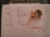
I'm trying to wrap my head around a transformer used in a circuit. It seems the schematic is some old school stuff and I can't get a clear picture of how the windings are arranged and which belongs to primary and secondary etc. I tried to post much of the circuit as I could to see if someone here can draw the transformer. To me it looks like W2, W1, and W3 are the Primary and the rest is all Secondary, but I'm confused.
 
Last edited:
I would have thought W1, W2 and W3 are secondary windings feeding half-wave rectifiers and smoothing caps. W4, W5 could be a split primary for dual-voltage use?
 
I agree with alec_t. w2 and w3 looks to be two half wave rectifiers set up in series. w1 looks to be imposing an ac voltage on top of the DC created by w3.

could w7 be the primary?

drkidd, you say this transformer is used in a circuit. What is the circuit for, what input voltage does it have? do you have a schematic for the circuit?
 
I'll share the contents of the PM so that everyone can have a look.
I've attached the slightly bigger circuit schematic and also the datasheet for the IC seen in the schematic.

From my interpretation of the circuit, W1 is the primary winding. W3 provides the High side voltage for the half bridge driver. while W2 provides an offset for the primary winding so a full swing from 400V to 0V can be achieved.

The initial high side voltage is provided by the AC input via a diode which is then reverse biased as soon as the 400Vdc is set-up. I'm not sure what the AC input is but Vcc is clamped to 15.6V, presumably R91 is correct to limit power dissipation in the IC. Because Vcc is clamped I suspect the rise time of this power supply is several cycles as it will take time to fully set up the primary offset and high side drive.
 

Attachments

  • Transformer.png
    Transformer.png
    88.8 KB · Views: 260
  • ir21531.pdf
    217.4 KB · Views: 258
Thinking about it further my above explanation doesn't totally work, as it doesn't explain where the power has come from. I think 400Vdc must be supplied somewhere, perhaps if we can see more of the circuit? It might be from rectified mains voltage perhaps?

Using rectified mains allows you to use a higher frequency driver (such as in this circuit) to minimise the required size of your magnetics (transformer).
 
Yes, the 400VDC comes of a rectified mains with PFC control. I think it's at about 65kHz frequency. So what I'm trying to do is get a clear picture in my mind of how this transformer is constructed because as it is I'm having trouble figuring out all the pieces.
 
Power factor correction?! What kind of power is this outputting, must be quite a large inductive load to require PFC.

So considering the 400V is coming from rectified mains I'm not really sure what w2 is doing. I can only think that it's there to provide additional regulation of the 400V, perhaps the rectified 400Vdc can dip slightly due to the comparatively low frequency of the mains and w2 can help mitigate this.
Either way w3 is your offset voltage and w1 is your primary winding.

What exactly are you wanting to know about your transformer? You say you would like to know how its constructed, is that just turns ratio or are you interested in the magnetic core ( inductance, material, geometry, winding layers)

Can you post a photo of the transformer?
 
What I want to know is which winding belongs where so that I can test and determine the turns ration etc.Basically like the below example so I can move on to my next step.
acpwrsup.gif


The input and PFC circuit is similar to the one in figure 1 of attached App Note.
 

Attachments

  • AN-8027.pdf
    843.1 KB · Views: 347
Look for little numbers written on the wires. Once, I went What when i saw about 25 black wires going to a connector. Then I found that they were marked every 6 inches or so with a number.
 
This is what the transfoer looks like. I was able to take it out the board. I took the magnets off as well. I measured the continuity of every lead and that's what I came up with.
 

Attachments

  • Transformer.jpg
    Transformer.jpg
    1.2 MB · Views: 183
Not sure What you expect to do with this transformer?
But it is Obviously made for a High Frequency Application.

I took the magnets off as well.
Not Magnets. They are Ferrite Cores.
 
Howdy, looks like a direct drive voltage multiplier. I'm not seeing the feedback for an SMPS.
I am seeing a big power driver pushing the transformer through 1,2 & 3 to get 400V center tapped. The 8V & 30V windings are along for the ride. G.H. <<<)))
 
I'm trying to get familiar with the gate driver a well since I don't any experience with them. What's the purpose of Q28 and Q30 just before the Mosfets Q29 and Q31? Also the IR21531 has what it seems 2 input voltages for Vcc, AC+ (which is the rectified voltage @~400Vdc) (R91 = 332K, R92 = 82K) and 12V going throuhg D39. Any ideas?
C62 = 1500pf and R98 = 9.1K which give an Fs of about 50Khz.
 
Status
Not open for further replies.

Latest threads

Back
Top