Futterama
Member
Hi forum,
I'm building a high-current 3-phase brushless motor controller and have found a high & low-side gate-drive IC and N-channel MOSFETs for the circuit (see bottom for links).
Circuit details:
The gate-drive IC uses bootstrap operation and can supply 4.5A source/sink gate current.
VCC = 15V
VDC (voltage to the load) = max 42V (10S LiPo cells)
Max load current = 200A
MOSFETs in parallel to handle high current = 4
I have read the datasheet and this application note AN-6076:
https://www.electro-tech-online.com/custompdfs/2013/08/AN-6076.pdf
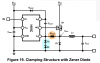
I think I have come to the conclusion that the circuit in figure 19, page 7 would be the best way to design my circuit (attached).
I'm trying to follow the AN when calculating bootstrap capacitor and gate resistor values but the AN has a bit bad english and the calculations makes little sense to me.
If I was to calculate the gate resistor, I would calculate the resistor value needed to limit the current to 4.5A at 15V = 3.33ohms. But when calculating it using the formulas in the AN, I get 57.7ohms.
Using the AN to calculate the switching time gives me ~95ns (4 MOSFET gates in parallel with each 107nC max and 4.5A drive current). But later there is another calculation where the sink and source current capability of the gate driver is calculated and they use a 1.5 factor. So now the switching time is suddenly ~143ns as the gate-drive current is "reduced" to 3A.
The switching time is not really important to me (of course it should be as low as possible) but I only calculated it so I could work with the rest of the calculations in the AN.
Besides the gate resistor and bootstrap capacitor values, I don't quite get the rule about sizing the zener diode for the Vs clamp. The AN gives me this:
"The Zener voltage must be sized according to the following rule: VB - VS < VBS,ABSMAX"
Does this mean the zener voltage must be lower than the largest negative voltage spike the drive IC can handle on the Vs pin (which should be 6-VCC = -9V)?
I haven't even begun to calculate the bootstrap capacitor value. I have been looking through another AN and was overwhelmed by the calculations and it seemed hard for me to figure out all the values in the calculations: https://www.electro-tech-online.com/custompdfs/2013/08/AN-9052.pdf
When calculating, I use a spreadsheet where I use 1 cell for each input value with a good explanation of the value and 1 cell with the calculation. I wish the AN's had such a spreadsheet attached.
Any help with these calculations for my circuit would be much appreciated")
Gate-drive IC:
Fairchild Semiconductor FAN7190_F085
Datasheet: https://www.electro-tech-online.com/custompdfs/2013/08/FAN7190_F085.pdf
MOSFETs:
Fairchild Semiconductor FDMS86500DC
Datasheet: https://www.electro-tech-online.com/custompdfs/2013/08/FDMS86500DC.pdf
I'm building a high-current 3-phase brushless motor controller and have found a high & low-side gate-drive IC and N-channel MOSFETs for the circuit (see bottom for links).
Circuit details:
The gate-drive IC uses bootstrap operation and can supply 4.5A source/sink gate current.
VCC = 15V
VDC (voltage to the load) = max 42V (10S LiPo cells)
Max load current = 200A
MOSFETs in parallel to handle high current = 4
I have read the datasheet and this application note AN-6076:
https://www.electro-tech-online.com/custompdfs/2013/08/AN-6076.pdf
I think I have come to the conclusion that the circuit in figure 19, page 7 would be the best way to design my circuit (attached).
I'm trying to follow the AN when calculating bootstrap capacitor and gate resistor values but the AN has a bit bad english and the calculations makes little sense to me.
If I was to calculate the gate resistor, I would calculate the resistor value needed to limit the current to 4.5A at 15V = 3.33ohms. But when calculating it using the formulas in the AN, I get 57.7ohms.
Using the AN to calculate the switching time gives me ~95ns (4 MOSFET gates in parallel with each 107nC max and 4.5A drive current). But later there is another calculation where the sink and source current capability of the gate driver is calculated and they use a 1.5 factor. So now the switching time is suddenly ~143ns as the gate-drive current is "reduced" to 3A.
The switching time is not really important to me (of course it should be as low as possible) but I only calculated it so I could work with the rest of the calculations in the AN.
Besides the gate resistor and bootstrap capacitor values, I don't quite get the rule about sizing the zener diode for the Vs clamp. The AN gives me this:
"The Zener voltage must be sized according to the following rule: VB - VS < VBS,ABSMAX"
Does this mean the zener voltage must be lower than the largest negative voltage spike the drive IC can handle on the Vs pin (which should be 6-VCC = -9V)?
I haven't even begun to calculate the bootstrap capacitor value. I have been looking through another AN and was overwhelmed by the calculations and it seemed hard for me to figure out all the values in the calculations: https://www.electro-tech-online.com/custompdfs/2013/08/AN-9052.pdf
When calculating, I use a spreadsheet where I use 1 cell for each input value with a good explanation of the value and 1 cell with the calculation. I wish the AN's had such a spreadsheet attached.
Any help with these calculations for my circuit would be much appreciated
Gate-drive IC:
Fairchild Semiconductor FAN7190_F085
Datasheet: https://www.electro-tech-online.com/custompdfs/2013/08/FAN7190_F085.pdf
MOSFETs:
Fairchild Semiconductor FDMS86500DC
Datasheet: https://www.electro-tech-online.com/custompdfs/2013/08/FDMS86500DC.pdf