Continue to Site

Welcome to our site!

Electro Tech is an online community (with over 170,000 members) who enjoy talking about and building electronic circuits, projects and gadgets. To participate you need to register. Registration is free. Click here to register now.

  • Welcome to our site! Electro Tech is an online community (with over 170,000 members) who enjoy talking about and building electronic circuits, projects and gadgets. To participate you need to register. Registration is free. Click here to register now.

How to identify PCB trace

Status
Not open for further replies.

jab99407

Member
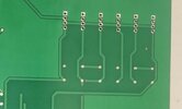
I don't understand the traces in the PCB layout, how are they connected. The diagram I have attached is a two layer PCB and I don't understand how traces are connected on PCB layout

Which pads are connected to the ground plane in a PCB layout?
I guess the top six pads are connected to the ground pen

are there Pads that only connected to a single trace?
 

Attachments

  • IMG_20220601_200602.jpg
    IMG_20220601_200602.jpg
    150.7 KB · Views: 284
If this is an empty PCB, I'd guess ohming the tracks is the easiest way to map them.

But if an empty PCB is all you can show, then that's pretty much it and nothing more. If this is somehow due to reverse engineering, then it's important to label each connected tracks - and then later on you may figure out bu using a pivot table in a spread sheet.
 
In the picture below, the pads in the red circles are connected to the ground plane by thermal reliefs. A thermal relief is used to make soldering easier.

In the blue circles are vias connected to the ground plane. They may be to connect a surface mount component on the other side of the board to ground or they might be for tying a plane on the other size of the board to the ground plane. This is often done to provide heat sinking by the large ground plane area.

PCB_copper_pour_thermal_pads.png


On your board, I'd guess the top set of patterns is for a row of 4 pin connectors. The top row is connected to the ground plane. The pins in the third row are connected together (power maybe), and the 4th row pins have tracks that lead off to somewhere. The second row of pins probably have individual tracks going somewhere on the other side of the board.

The short horizontal tracks in the middle of the board either have components connecting them on the other side of the board or may be vias, with tracks connecting between the blank areas on the other side of the board.
 
Status
Not open for further replies.

Latest threads

New Articles From Microcontroller Tips

Back
Top