Electro Tech is an online community (with over 170,000 members) who enjoy talking about and building electronic circuits, projects and gadgets. To participate you need to register. Registration is free. Click here to register now.
Welcome to our site! Electro Tech is an online community (with over 170,000 members) who enjoy talking about and building electronic circuits, projects and gadgets. To participate you need to register. Registration is free. Click here to register now.
I've always gotten the best results using the photoetch method. I used to spray coat my own boards with photoresist, but: a) it's a real pain to get the coating perfect & free of defects, b) GC electronics doesn't make the spray resist anymore. So I use positive-acting presensitized boards now. Also, instead of printing my artwork onto film myself (which doesn't work all that bad), I print finished artwork on paper at 2 times scale, then take it to a local graphic arts guy (who makes decals, bumper stickers, etc.) who photographically reduces the art to 1x onto film for me. The traces and pads on his films are very opaque with NO pinholes. He charges me $6US per shot, and I think it's worth it. I get the results I'm looking for.
JB
If you are using the laser printer- transfer method, practice, practice, practice. I make a sandwich between two pieces of glass and put a piece of cotton cloth over the paper. I use metal spring clamps to hold it all together and put it in the oven. The oven is set on pre-heat to 400 degrees F. As soon as the temp hits 400, I take it out and let it cool, then soak the paper off. I print on the pasted side of prepasted wallpaper, which soaks off easily.
Allow for some spreading of the ink in your layout, 10 mil spacing won't work. I can layout TSSOP packages, but don't do it if possible.
This is my latest layout:
Hi Monkeytree, as I said in the other topic, I'll now go through how I do my boards. It's going to be long, but I hope it helps you. It'd be handy to know which country you are in, because I can tell you then where I get my board from, etc., it's the best board I've used so far and has allowed me to get incredible results for the first time.
First thing I do is draw my schematic in Eagle, available in a free version which is what I'm using, with limited board size (fine for most hobby circuits) from www.cadsoft.de.
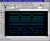
I then change to the board layout part of the program and set out the components, which I move around as I'm routing it. If using the autorouter, I save it before autorouting so that if I need to change things to get it to route better, I can reload the unrouted layout. Here's my present project after I've manually routed the entire board (autorouter isn't always very good):
**broken link removed**
It's then ready for printing. I use Staedtler Lumocolor Inkjet Film (Transparencies), grade 0.10mm, part number: 639 30 A4 H. They work very well. My printer is an old Epson Stylus Color 740 and is capable of maximum resolution of 1440x720 dpi. In the printer preferences, I choose print media as Photo Paper, and set it to the highest resolution (as if printing out a photograph on to glossy photo paper). In the Eagle print settings, I make sure I choose 'mirror' so that the layout prints out mirrored, since the view in Eagle is from the top of the board. I then print out the layout 3 times, using a splicer to cut off the print-out from the A4 transparency sheet each time, so the print-out doesn't go through the printer again and get smudged to death. Each time cutting off more of the sheet, so when overlayed the pieces of transparency get smaller and thereby give room for sellotape to stick each one to the one below. They must be precisely positioned over each other, especially if there are tracks close together. Here are the three of them overlayed and stuck together:
**broken link removed**
Now for the board. I use pre-coated photo-resist board from www.maplin.co.uk (in the UK, hence why I wondered where you live), which seems to be excellent. I cut it to the correct size, peel off the protective plastic over the copper and then quickly position the transparency over it. Then I place a piece of glass from a photo frame over the lot (heavier the better) and, using a couple of plastic can tops from my foam cleaner and freezer spray, place a UV face tanner over it all, so the UV source is about 3 inches above the board. I used a test strip and exposed patches for different times to find out what was needed - 1 minute exposure didn't quite do it, but 2 minutes and above was perfect, so I expose for 2 minutes using a countdown timer. Here is the face tanner I use (it's my wife's, she's very lenient and accepting of me ), cos I can't afford £100+ for a little PCB UV box when I make, what, one board a year?
**broken link removed**
After exposure, unlike some photo-resist boards I've used, you can't see any hint of the layout on the board yet really. I quickly take the exposed board into my developing room (the kitchen... oops, I've already got some chemical or other on the stainless steel sink, which is now stained steel, and my wife was not overly impressed. I can't help being a mad scientist at heart!) and dunk the board into a tray of Carbonate-based developer. Rocking it back and forth constantly, I stand there and forget timing it, I just watch until I can see the layout magically appear and carry on until there is no photo-resist left between close-together tracks, etc. My developer is a bit past its best now, and it takes around a couple of minutes till I'm happy it's done. Doesn't much matter, I could leave it in there for 5 minutes and it wouldn't over-develop, Carbonate is so much more gentle than the caustic soda (Sodium Hydroxide developer) I used to use back in the day.
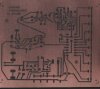
When that's done, I rinse the board and place it in warm Ferric Choride solution, and stand there rocking it for as long as it takes, sometimes 20 minutes or so - boring, but it makes it etch faster. Sometimes I pour the acid back into my jug and warm it some more in the microwave (how long till the inside of the microwave has disappeared, I wonder, and how will my wife react... ho hum) and then pour it back into the tray. Speeds things up no end. Having dried the board, I get my little 12V PCB drill out and start drilling the holes, which is easy thanks to Eagle leaving a hole in the middle of each pad, so the copper gets removed there, giving a simple reference point for drilling, and making it easier because the drill can bite straight into the board material without swirling around on shiny copper, trying to get a grip and cut. In fact, the comparitively hard copper actually acts as an auto-centre to push the drill bit towards the centre of the pad. Here's the board after etching and drilling:
**broken link removed**
Then it's simply a case of populating the board and soldering everything in place. I print out a non-mirrored image of the board with components showing but not the tracks - as they make it hard to see the parts and values properly - and then use that to see exactly where I need to place components, and their respective orientations. Here it is with parts soldered in place:
**broken link removed**
And from the top, complete with ugly looking cables running to the speakers and audio output on the soundcard, along with a large heatsink bolted to the IC:
**broken link removed**
So there you have it. If you're still with me and haven't flat-lined or fallen, snoozing, to the keyboard, this might help you or anyone else to obtain good results. I've been doing boards for around 7 years now, and these are the best I've ever managed, so it's been quite a course of trial and error, I'm just glad that I finally discovered this method and good board from Maplin.
thanks for the advice, and i did not fall asleep i had been using Ferric chloride etchant from www.rapidelectronics.co.uk (tools and production equipment) i got the wrong stuff
I make double sided boards using the positive photoresist PCB, I thought double sided would be very difficult to line up but it isn't it is actually pretty simple.
Using my PCB program I print out the two sides on transparencies with my laser printer (no smudging and crisp lines) then place the two side, toner side in together and line them up while looking through them, tape them together making a pocket(one side untaped), slide your board in the opened end then tape it shut. Carefully place the board in between two sheets of either glass or thick plastic and tape them together, this will sandwich everything and help stop it from moving. Place it under the flourecent lamp for 5 min on each side, remove and develop. Then etch using your etchant, I use Ferric Chloride in a jug with a heater and a small submersible pump to move the fluid around.
I have never had any problems even with surface-mount parts. if you get your toner density right, and your ironing technique down, you don't get much spreading of the toner during transfer so you can get away with very fine traces (yes, even 10 mil spacing)
note that one main difference between my method and "the usual" method is that I set my iron to only 2/3 heat, rather than all the way. For those of you who routinely do toner transfer, I suggest you give that a try at least once... since I've started doing it that way i've had 4 boards in a row come out perfect (one rather large one, see the pics on my tutorial page), with minimal trace spreading or blobbing, and few to no broken traces, etc.
Also, I use a totally different etching method than most. I prefer sodium persulphate over ferric chloride because it's almost as fast, but it's crystal clear so you can really see the progress. I do my etching in a ziplock baggie, which allows me to use a very minimal amount of etching solution (1/4 cup of water, a couple tablespoons of powder usually) and also allows me to agitate the solution by hand, and focus on areas that are etching slowly. and when I'm done with the solution, i can just dump that tiny bit down the toilet and throw away the bag.
I do the exactly the same an Handyman.
Will never use any other method.
I use universal developer-Sodium dydroxide Free
It's from www.rsaustralia.com cat. no. 690-849
This developer does not have aggressive over-developing characteristics of Sodium Hydroxide developers
It's expensive but so gentle.
Hanyman, what version of Eagle do you have? I have 4.13r1 and it does not have holes in pads, which makes drilling difficult. Also, the print function does not work. I thought it was something left out in the free version, but maybe I just don't know how to do it?
I have 4.13r1 also. Do you mean the pads on the screen do not appear to have holes? Mine are on screen and present when printed out, even if the track I lay seems to cover the hole on the layout.
The print function works for me, although I found that it seems quirky, and to get mine to print at all, I always have to click on 'printer' within the print dialogue box and then pretend to change the printer settings, etc., before clicking on 'OK' and 'Print' which then takes me back to the original box. When confirming the job in that box, it starts printing properly. Otherwise it will claim to be doing the print job but nothing will happen at the printer end.
Thanks for the reply, yes, no holes any time. The printer problem is the same with me, I had not figured out how to make it work. I have been in contact with Eagle email help, I will ask about the pad holes.
Ferric chloride user, how do you get the rust stains off everything?
If the answer is hydrochloric acid, where do you get it from?
Anyone know where ammonium persulphate cn be obtained?
I use Ferric Chloride and don't have rust stains on anything except the tub I use for etching and the old measuring jug I use to pour the solution back into its bottle.
If the answer is hydrochloric acid, where do you get it from?
Well, when I lived in Spain, every supermarket stocked it for cleaning purposes, cos they don't see the need to mollycoddle their population, afraid they're so dumb they'll hurt themselves with something as dangerous as a concentrated acid... but here in the UK, we are too dumb to be allowed to buy such a thing as hydrochloric acid, so I can't help with where to obtain in from in concentrated form. However, there is a kitchen cleaning spray known as Cillit Bang which claims to remove limescale very quickly. I guessed it may use very weak hydrochloric acid in it to do the job, so I mixed some with Hydrogen Peroxide and stuck some copper-clad board in it overnight. In the morning, the copper was gone, so it looks like it does contain HCl.
Anyway, a search on Google brings up a solution which claims to be purely for the removal of Ferric Chloride stains...
**broken link removed**
which uses Oxalic Acid.
Anyone know where ammonium persulphate cn be obtained?
Thanks for the reply, yes, no holes any time. The printer problem is the same with me, I had not figured out how to make it work. I have been in contact with Eagle email help, I will ask about the pad holes.
Hydrochloric acid is also known as muriatic acid. It's used to [thoroughly] clean masonry, concrete etc. You might check at a local hardware store or building supply center (your location isn't listed though).
JB
This site uses cookies to help personalise content, tailor your experience and to keep you logged in if you register.
By continuing to use this site, you are consenting to our use of cookies.

 ), cos I can't afford £100+ for a little PCB UV box when I make, what, one board a year?