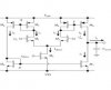
This is a long tailed pair. Here goes:
Put a bias voltage on VBIAS. This causes a current to flow in the drain of M5. This current is split between M1/M3 and M2/M4. If the input voltage Vin+ exceeds Vin-, then all the current flows down the M2/M4 combo. M4 and M6 form a current mirror. If they have the same turn on voltage the current i2 should be equal to current i6. Current i2 creates a certain gate-source voltage (=VDD - Y) and if M4 and M6 are matched, since this same gate-source voltage is applied to M4 and M6, equal currents flow. Likewise with M3 and M8. Therefore by changing Vin+ - Vin-, you can change the amplitude of i2, hence the amplitude of i6. Likewise with i8 and i7, so Iout is equal to i6 - i7.