Continue to Site

Welcome to our site!

Electro Tech is an online community (with over 170,000 members) who enjoy talking about and building electronic circuits, projects and gadgets. To participate you need to register. Registration is free. Click here to register now.

  • Welcome to our site! Electro Tech is an online community (with over 170,000 members) who enjoy talking about and building electronic circuits, projects and gadgets. To participate you need to register. Registration is free. Click here to register now.

how 4017 to produce the negative output decoded pulses

Status
Not open for further replies.

cuusinhvien

New Member
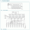
Does any one help to wire the counter IC 4017 to generate the negative pulse output since the input is clock signal.

I had found somewhere on the internet before but forgot, that the clock signal fed into the pin 15 or 13 ... and pin 14 to ground then outputs will produce negative decoded pulse???? correct me if I am wrong.

Thanks so much

CSV
 
Hi,
If Pin8 is at 0V and pin12 is at +V.

The 4017 will produce a high going 'positive' pulse on the decoded output.

Why would you require a 'negative' pulse.?
 

Attachments

  • AAesp01.gif
    AAesp01.gif
    34.6 KB · Views: 324
I need the negative pulses to drive the P-channel FET in the high power flashing circuit.

What does it mean "The 4017 will produce a high going 'positive' pulse on the decoded output" ?? my understand that the positive pulses are already done in the traditionnal diagram of 4017 IC. Or you have some advaced idea to advise.

Thanks

CSV


'
 
Last edited:
Hi,

the CD4017 counts at each high edge of the clock pulse incrementing the outputs to be high in sequence.

To drive a P-channel MosFet transistor the counter outputs must be inverted.

This can be done by inverting the counter output signals.

An easier way would be using N-channel MosFet transistors. N-channel MosFet transistors have the advantage of a much lower RDS(ON) than P-channel types.

Boncuk

Thanks Boncuk

- The state "...inverting the counter output signals" is what you mean if using P-channel mosFET? (attached 1)

- And the attched 2 is that possible idea if using N-channel mosFET?

Please advise
 

Attachments

  • Pulse convert P-channel mosFET1.JPG
    Pulse convert P-channel mosFET1.JPG
    14.8 KB · Views: 286
  • Pulse convert N-channel mosFET.JPG
    Pulse convert N-channel mosFET.JPG
    14.6 KB · Views: 275
hi cuus,
I guess when you said 'negative' pulses you really meant low going pulses. ie: from high to low, +V to 0V............?

Look at the CD4049 hex [6] inverting buffer.

You could use a N MOSFET connected to the 4017 outputs, place the load in the Drain of the FET.
 
hi cuus,
I guess when you said 'negative' pulses you really meant low going pulses. ie: from high to low, +V to 0V............?

Look at the CD4049 hex [6] inverting buffer.

You could use a N MOSFET connected to the 4017 outputs, place the load in the Drain of the FET.

Right! "from high to low"
good idea with CD4049, but more component to be crammed to the circuit.
Does any disadvantage if load's placed in the Source of N-channel mosFET?

Thank you in advance

CSV
 
Right! "from high to low"
good idea with CD4049, but more component to be crammed to the circuit.
Does any disadvantage if load's placed in the Source of N-channel mosFET?

Thank you in advance

CSV

The advantage of the load in the Drain, is that the Gate voltage can be less than the Load voltage.

eg:
say the FET Gate required a +5V to be turned ON, the Load could be connected to +12V.

If the Load was in the Source lead the +5V on the Gate would not fully turn on the FET, because of the voltage drop across the load, which would try to pull up the Source pin.

Do you follow that OK.?

If I understand, you want the High on the 4017 pin to turn OFF the current to the load.??

So all the Low pin loads would be ON, is that correct.?

Whats the load voltage supply also the 4017 supply.???
 
Last edited:
So your load must be on ground.
If the load is connected to the source of a N-FET then the source will be about 5 volts below the gate. Gate=12V and Source = 7V.
 
Now I've got it

Infact my existing circuit is similar way to drive the power transistor and load feeding by 0V as motocycle electronic flashing unit (attached)

So that's why I need to replace the NPN power transistor Q2 by P-channel mosFET, but somebody advised the N mosFET is better. Power Supply is also 12VDC.

CSV
 

Attachments

  • Flashing circuit.JPG
    Flashing circuit.JPG
    20.8 KB · Views: 196
Last edited:
Now I've got it

Infact my existing circuit is similar way to drive the power transistor and load feeding by 0V as motocycle electronic flashing unit (attached)

So that's why I need to replace the NPN power transistor Q2 by P-channel mosFET, but somebody advised the N mosFET is better. Power Supply is also 12VDC.

CSV

BTW my attached diagram is showing the motorbike turn flashing signal circuit to replace the traditional thermal flashing relay, so that why they hook the ground supply via loads (following the original concept of manufacturer), but as my experiment the circuit did not work well because when Q2 is on, the voltage at Emitter come up nearly with Vdd so cause the oscilation of Q1 is fail to supply and the flashing pace is disorder...
So I wonder if sombody help to solve this problem but keeping the traditional connection or have some good idea to improve it.

Thank so much

CSV
 

Attachments

  • Flashing circuit.JPG
    Flashing circuit.JPG
    20.8 KB · Views: 172
Status
Not open for further replies.

Latest threads

New Articles From Microcontroller Tips

Back
Top