Electro Tech is an online community (with over 170,000 members) who enjoy talking about and building electronic circuits, projects and gadgets. To participate you need to register. Registration is free. Click here to register now.
Welcome to our site! Electro Tech is an online community (with over 170,000 members) who enjoy talking about and building electronic circuits, projects and gadgets. To participate you need to register. Registration is free. Click here to register now.
I am designing a High Speed Operational Amplifier using LT spice for my project. Planing to use Miller op amp. Kindly advice me what are the amp (part #s) should use for 3 stages? I am new to LT spice
I am designing a High Speed Operational Amplifier using LT spice for my project. Planing to use Miller op amp. Kindly advice me what are the amp (part #s) should use for 3 stages? I am new to LT spice
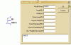
Attached schematic is my proposed Miller op amp design. I have drawn it on LT spice. I used BSIM 3/ NMOSs and PMOSs, But It did not work. I can not get open loop gain and output swing. Do I need to key in gama, Cox, etc? I only keyed in ‘W’ and ‘L’ values for the transistors. If that so where to key in them in LT spice? I know winspice , we can use .txr file to enter values.
Thanks Eric
I should meet some specs like differential to single gain >1000 and CMMR> 75dB and few more. Still ongoing lectures in campus, like freq responses. I also need to compare theoretical values with LTspice simulation values. That is why I can not use known MOSFET from the library. I am still reading my theory, must submit the report by mid nov. I will post my final .asc, once I submit the report.
My first specs should meet Differential to single-ended gain > 10k
I did set a common DC voltage of 1V at both inputs (to bias the devices). Then
Kept one of these DC voltage constant and done DC sweep of the other input voltage.
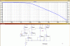
I got the Vout vs Vin plot. Taking the differential of that plot, I got the Gain vs Vin. With those 2 plots, I did generate the Gain vs Vout plot which is required. See the attached .doc file.
In that plot, I got to draw a horizontal line corresponding to a gain of 10k. The 2 intersecting points will determine the output voltage swing. Hence, this plot will reveal whether I have achieved a gain of 10k while maintaining a minimum voltage swing of 1V.
But my problem is I can not get required voltage swing of 1V at 10k gain. Mine was less a than 1v . As I have power supply of 1.8 v . I should be able to get more than 1V of swing?
hi,
Download your files, looking, get back to you.
EDIT:
You have not included the B3SIM.lib
ED2: what is the real world equivalent to those FET models, it one doesn't exist there is little point in designing your own OPA circuit.???
As you mention “The output stage M5/6 requires the CC source and biasing to be redesigned”
Do I need to do it for DC biasing too? How do I do it? Remove the resister and add PMOS would help?
Your proposed approach would help me to meet rest of the specifications, I guessed. I should find single ended gain with DC sweep first. Then find CMMR >80db once the circuit meet the first specs. (Gain >10)
Later on, when amp in closed loop and with 1pf load cap, need to find out put voltage swing >1 peak to peak. Gain peaking should be lesser than 3 db. etc. I am confused. How much I read also unable to apply to this practical situation. I am using Razavi’s text book too.
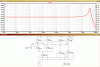
I have modified my circuit as your advice. So I can meet my specification which is gain more than 10k while maintaining Vout 1Volt swing. Please see the specs1.asc file and .doc file. (Please note my Vdd and Vdd1 are +.9 and -0.9)
From that I can go and find my 2nd specification which is to find Acm when both V1 and V2 connected together and do DC sweep. See the Specs2.asc file (Please note my Vdd and Vdd1 are +.9 and -0.9)
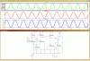
Next for specs 3, I should do Transient analysis. See the specs3.asc. I should give 1V p-p sine wave with 1V dc input and get 1v p-p output when the amp in close loop.
My issue is in specs3 I can not use Vdd and Vdd1 are +.9 and -0.9. But is use Vdd and Vdd1 are 0 and 1.8 I can get both input and out put 1v p-p.
Please tell me why I can not use Vdd and Vdd1 are +.9 and -0.9 for specs3? Is my Transient analysis circuit wrong?
This site uses cookies to help personalise content, tailor your experience and to keep you logged in if you register.
By continuing to use this site, you are consenting to our use of cookies.