Continue to Site

Welcome to our site!

Electro Tech is an online community (with over 170,000 members) who enjoy talking about and building electronic circuits, projects and gadgets. To participate you need to register. Registration is free. Click here to register now.

  • Welcome to our site! Electro Tech is an online community (with over 170,000 members) who enjoy talking about and building electronic circuits, projects and gadgets. To participate you need to register. Registration is free. Click here to register now.

High speed MOSFET switching and stability problem

Status
Not open for further replies.

SAnton

New Member
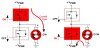
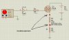
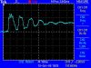
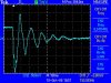
Hello! I`ve got some problems with fast MOSFET switching. My design is high-speed square-wave pulse generator with nanosecond rise and fall times, where MOSFET acts as a switch. I`ve searched several fast-switching FETs, and found that IRF630N is really suitable for my design. It has good characteristics (Turn-On Delay Time 7.9ns, Rise Time 14ns, Turn-Off Delay Time 27ns, Fall Time 15ns), then I decided to drive FET with IR4427. External signal generator parameters 0-20kHz with 100ns rise and fall times. When I connected generator with a MOSFET driver, I`ve got better pulse response, IR4426`s output showed 50ns rise and fall times. I thought that it is very good and my problem is solved until I connected IRF630N to the output of the driver through 10Ohm resistor.
I found it terrible, there were so much unwanted oscillations through the load.
What can be the problem? Circuit and oscilloscope snapshots attached. Thanks..
 

Attachments

  • 1.JPG
    1.JPG
    41.7 KB · Views: 1,207
  • rise.JPG
    rise.JPG
    63.9 KB · Views: 810
  • fall.JPG
    fall.JPG
    66 KB · Views: 822
Place your 68 ohm resistors on the mosfets drain. Then apply at least 7v preferably 10v to the gate.This way you will drop about 23v across the 68R and about 2v Across the 4.7 ohm resistor Dont exceed 20vgs your FET can only take 20Vgs! Or use a P-channel FET. You are using an N-channel Fet as a highside switch.
 
Last edited:
the load resistor (4Ω7) too.
 
Forgot to add why are you using such a large FET for about 200mA pulsed current. Depending on your frequency and duty cycle you may be able to use something like a NTS4001 or 27002. You could switch these at about 30nS easy with a your driver.

Boncuk his pic shows a diff measurment across the 4.7 ohm resistor I'm guessing whatever he is interfacing too cant tolerate 25V.If he leaves the 4.7 ohm resistor there his signal will be about 2V.

Edit

Sorry Math error.

343mA x 4.7R = 1.6V.
 
Last edited:
Thanks for attention! I increased values of resistors during the experiment. There were 10 Ohms resistors, but they were becoming too hot! Approx. 0.2-1A may be needed in this circuit.
--May be these oscillations come from the power supply unit? In ideal conditions I need to get sharp rise and fall, and clean pulse width.
 
You can’t drive an N-Channel Fet with the load on the source like that, unless you use a High Side driver or isolated drive.

You are turning the fet on/ off by raising the source up to the gate potential that is why you are seeing oscillations. Put your load on the drain!

Do this

**broken link removed**

OUTPUT

**broken link removed**
 
Ok! I`ll try as soon as possible.
Another question: there`re voltage surges on signal rising and falling, is it can be eliminated?
(As I understood you are using Proteus?)
 
To suppress the leading edge spike the simplest method is to RC filter it,this will slow down your signal (rise/fall). There are active circuits to blank it out used in PWM controllers for SMPS. You can search Google "spike leading edge blanking".

First test it on a breadboard and see if it's acceptable.

Here is an example of a discrete LEB (Leading Edge Blanking) from EDN. I've never tried it. Starts on page two.

Code:
http://www.edn.com/contents/images/52903di.pdf

Here is a cut and paste of what causes it.

"A general problem with detecting the current flowing through the switched terminal of these gate-driven semiconductor devices is that in the process of turning the device ON, a charge current flows into the gate terminal, out of the reference terminal, and through the sense resistor. As this charge current flows through the sense resistor, a voltage appears across the resistor. Since that voltage is generally present only during a short portion of the full time that the device is ON, it is considered to be a voltage spike. Whereas it is desirable that the voltage waveform across the sense resistor be representative of the current flowing through the switched terminal of the semiconductor device, the voltage spike appearing across the sense resistor represents a deviation from the desired waveform. This voltage spike can present problems in many circuit applications. While attempts have been made to filter the voltage spike, the filtering itself tends to create additional problems."


I used Pspice to simulate the circuit.
 
I`ve got another problem:). How to open low-side (lower) MOSFET, if the source of it connected to negative polarity power supply as follows in attachement.
 

Attachments

  • 1.JPG
    1.JPG
    22.8 KB · Views: 657
Status
Not open for further replies.

Latest threads

New Articles From Microcontroller Tips

Back
Top